
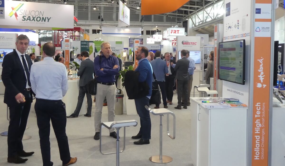
The trade show floors at the combined SEMICON Europa and Productronica events can be daunting. In past years, we’ve focused our visits on the SEMICON Europa exhibitor floor, but as the lines fade between front-end processes, advanced packaging, and board assembly, getting the whole story called for visits to the Productronica halls as well. We had some great discussions about recent mergers, collaborative partnerships, and new product offerings designed to meet the needs of the technology megatrends described in the keynote talks. Let’s start off with a slide show and some general observations.
We were amazed at the sheer size of the stands at Productronica compared with Europa. For example, ASM Assembly booth occupied 800sq m. of space, with its own technology stage and agenda, a restaurant, and a complete demo line featuring the company’s expanded portfolio. The nearest to that in the SEMICON Europa hall was the Silicon Saxony stand, where numerous German-based companies were represented. In the past year and a half, ASM assembly has been snapping up advanced packaging equipment suppliers, such as Nexx and Amicra to broaden its capability in advanced packaging for automotive applications.
Productronica Innovation Award

the Productronica Innovation Award for the Semiconductor Cluster.
We stopped to talk with Johann Weinhandler, ASM Amicra, and congratulate him on winning this year’s Productronica Innovation Award for the Semiconductor Cluster, for the COS Die Bonder tool. COS officially stands for chip-on-submount, but Weinhandler said it really was a chip-on-chip assembly tool. It is designed specifically for photonics assembly applications, achieving 3µm placement accuracy and high-speed eutectic bonding. 20 years in the making, Weinhandler himself developed the high-resolution imaging and a dynamic alignment system that enables the tool to be used in high-volume applications.
Casting Wider Nets
ASM Assembly isn’t the only equipment supplier that has caught on to the need for casting a wider net to serve the electronics supply chain. KLA’s acquisition of Orbotech that was completed by SEMICON West has, in the words of Orbotech’s Lior Maayan, broken the chains of supply and created a new “supply net” that leverage both market and technology synergy of both companies, and also includes SPTS Technologies. In the process, Orbotech is no longer a publicly-traded company, and SPTS is no longer under the Orbotech banner. Both Orbotech and SPTS Technologies maintained their brands and carry the sub-brand: A KLA Company.
KLA is known for its front- and back-end metrology and inspection process control capabilities. SPTS provides wafer-level processing tools for advanced packaging etch, metallization, and dicing processes. Orbotech brings direct imaging lithography for redistribution layers (RDL) and defect inspection for PCB and substrate-like PCBs. Orbotech tools also feature AI-driven informatics software that allows defect, metrology and process data to be shared across platforms. Together, they represent the convergence of front-end, packaging and PCB metrology, inspection, and software.
“We are the first to go from the front end, through advanced packaging, to PCB,” noted Maayan. “We can now share know-how across the entire electronics manufacturing supply chain.”
According to Oreste Donzella, CMO of KLA, this puts the company in a unique position to strengthen in-line process control to provide end-to-end reliability, specifically targeting the automotive electronics market’s quest for zero-defects. He explained the importance of being able to share reliability data across the supply chain from the fab, through device assembly, and finally board-level test to conduct inline parts average testing (I-PAT) to find outlier chips. Outlier chips are those that have passed various tests as they move through the supply chain, but still fail due to latent defects.
Power Module Advanced Packaging
At Boschman, we got a lesson in the company’s core technology, pressure sintering, from Frank Boschman himself. This emerging die-attach technology offers a void-free strong bond with very high terminal and electrical conductivity. It targets power IC packaging for automotive applications. Boschman walked us through the fully automated process.
Advanced packaging at Boschman means replacing traditional solders with sintering materials for better performance and higher reliability. It also means replacing wire bonding with ribbon bond or clip bonding for better CTE match, higher thermal conductivity, and reliability. Lastly, it means improving geometry, especially for double-sided cooling, and reducing form factor to reduce cost.
We talk a lot about how automotive electronics are driving advanced packaging and heterogeneous integration, but in reality, 75% of automotive packages are still traditional wire-bond. While business is growing, Boschman says volumes are still low. They work with tier-one manufacturers and have also worked directly with the automotive OEMs, as is a growing trend.
Shock and Lock Solves Fan-out Warpage
Business is good at ERS, according to CEO, Klemens Reitinger. “We don’t see a downturn in advanced packaging,” he said. “Fan-out wafer-level packaging (FOWLP) is really growing.” This is the company’s sweet spot for its thermal debonding system, designed for warpage correction in advanced packaging applications; namely FOWLP. It is the second product in its portfolio. The first being thermal chucks for probe testers. The company has also developed a second system that can accommodate panel sizes up to 700 x 700mm.
Reitinger says he came upon the concept for the company’s “shock and lock” process quite by accident. He was removing a reconstituted wafer from the thermal chuck by hand, and it was hot, so he dropped it onto a cold chuck. The wafer flattened immediately.
Reittinger harnessed this eureka moment, patented the technology and trademarked it as AirCool™. The idea is to “shock” the reconstituted wafer with temperature so it “locks.” Different die requires different temperatures, explained Reitinger. The fully automated system can achieve throughputs between 20 and 40 wph. It is suitable for both eWLB and M-Series FO processes.
Solid Foundations
In an effort to achieve high accuracy and precision positioning, many tool manufacturers are limited by the effects of environmentally caused vibrations. Tim Anderson, of Integrated Dynamics Engineering, has a solution for that. It’s called an active dampening vibration isolation system. Commonly used in front-end applications for metrology, inspection and lithography tools, IDE has developed a version for back-end process tools.

“This is becoming an enabling technology for high speed, high accuracy pick-and-place for FOWLP, and in applications for moving large mass with high-precision positioning,” explained Anderson.
The system creates a floating base that is integrated into the tool to insulate it from vibrations caused by the tool itself, as well as external causes, such as road traffic. “It’s the part of the tool people don’t think about after the tool is designed,” he said. “Where the tool is placed on the manufacturing floor could impact it.” After we spoke with Tim, I started noticing how many other companies mentioned accuracy limited by a tool’s vibration.
Continued Expansion
I stopped by for my usual chat with Clemens Schuette, at EV Group. He told me the company is once again in expansion mode: adding new cleanroom space to its ever-growing campus in Schaerding, Austria. At SEMICON Europa, EV Group was promoting its recent collaboration with DELO, a leading manufacturer of industrial high-tech adhesives, to further develop its wafer-level optics and nanoimprint lithography capability. The goal of the collaboration is to speed up materials development cycles, to better serve the growing optical sensing market. You can read more about it here.
Copper on Glass Substrates
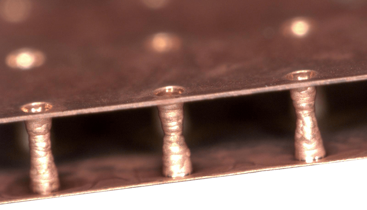
Plan Optik promised something new at SEMICON Europa, and they didn’t disappoint. The company’s big news was the introduction of an industry-first: pre-drilled, through glass via (TGV) wafers with an applied copper layer. The wafers are available in sizes up to 300mm, with hole diameters down to 100µm, explained Markus Wagner, marketing director at Plan Optik. Additionally, custom RDL patterning is available on wafers up to 200mm in size.
This is good news, as glass substrates are gaining traction in high-frequency applications, including 5G. Metallizing glass has been one of the big challenges. Wagner said while the first products introduced are copper coated, they aren’t stopping there. The process can be done with other metals, such as gold. Future plans include filled vias and glass circuit boards with integrated passive devices.
Japan is In the House
While Rorze was new to SEMICON Europa, the Japanese robot company is not new to the industry. Director of Sales, Patrick Julien, explained after years of using a local distributor, the company recently opened its European office in Dresden in 2019. They invented the clean robot, and many of the stockers and sorters you see on automated process equipment bear the Rorze brand.
Another Japanese exhibitor that especially caught our eye was the Tokyo Boeki Group, with its Minimal Fab Promotion Organization. Working on ½ inch wafers that produce one chip at a time (yes you read that right) the consortium has developed a full line of fab processing tools with the cleanroom atmosphere built into the tool. These tools are about the size and shape of an office water cooler. While Minimal Fabs are no match for mega fabs in terms of volume production, it is an interesting concept for development and low volumes. A full line can produce up to 40,000 chips/month.
Back over at Productronica, we spent some time at the Saki booth, learning about its inline 3D-CT automated X-ray inspection (AXI) system for insulated gate bipolar transistors (IGBT) power packages used in aerospace and military applications. As market trends call for deeper inspection of BGAs, the company identified a need for AXI tool that would tackle the most challenging defects, such as the so-called “head and pillow”. Saki’s unique planar CT technology makes it possible to analyze the internal structure of planar objects. Its detector uses a parallel movement to capture images from different directions and creates a tomogram. It features a “judgment station” that makes it easy to understand what the operator is viewing.
SEMICON Europa and Productronica Booth Parties
SEMICON Europa and Productronica would not be complete without the traditional booth parties. The official festivities kicked off Tuesday night with FRT’s annual party. The metrology company had lots to celebrate this year, with its recent acquisition by FormFactor. The deal caught many by surprise, as FormFactor’s core competency is electrical test, and FRT is based in optics for metrology and inspection. But according to both FormFactor CMO and director of M&A, Amy Leong, and FRT Founder and CEO Thomas Fries, it’s a perfect marriage. FormFactor was looking to expand its capabilities without overlapping, and FRT was looking for a way to help expand its global footprint. The best part: FRT will maintain its brand. After SEMICON Europa, I paid a visit to FRT’s HQ in Badisch-Gladbach. Look for the full story in our upcoming 2020 Yearbook.
Later that evening, we found our way to SEMI’s annual networking party, which took place at the swanky Bayrischerhof Hotel. It’s always a fun evening, connecting friends and meeting some new people.
Wednesday is the official party night, and we made the rounds: whiskey tasting at memsstar and its neighbors, saki at Rorsche, wine and cheese at Technic, and Belgian beer and specialty cocktails at Trymax. Sadly, we never made it over to the parties at Productronica, but we hear they are quite something. Like I said, trying to do it all is daunting. My advice – pace yourself and save some things for next year! ~ FvT


