
 The Electronic Design Process Symposium – EDPS 2919 – is known in the IC design community as a rather small (50 – 100 participants), but a highly interactive workshop. The 26th edition, hosted again this year by SEMI at its Milpitas headquarters, October 3 -4, 2109 featured both EDPS IC design experts and a growing number of manufacturing experts, who presented and discussed the latest innovations in the semiconductor industry and exchanged ideas how to further improve integrated circuits (ICs) and expand their reach.
After Intel’s Ramond Rodriguez, general chair of EDPS 2019, welcomed everybody, I had a difficult responsibility: Reminding all of us that our longtime friend and very supportive EDPS committee member, Camille Kokozaki, had died last April (Figure 1).
Design and Manufacturing Processes for Growing Markets
EDPS 2019 focused on efficient methods for design and manufacturing processes to achieve higher speed, more secure, and lower cost and power electronic solutions. Rapidly growing markets, like automotive, high-performance computing, 5G wireless, and wired communications demand more and more from our industry. Innovations in artificial intelligence (AI), machine learning (ML), photonics and advanced packaging were the main technology drivers presented and discussed to achieve these goals. Because all presenters’ slides will shortly be available at no charge here, allow me to focus the rest of this blog on the “Advanced Packaging” session on Thursday afternoon and the impressive dinner keynote.
Advanced Packaging at EDPS 2019
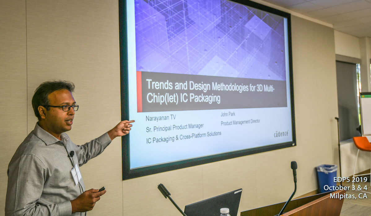
In my brief introduction to this session, I highlighted, as I always do, the importance of a well-functioning ecosystem, explained what the four speakers will address and how they complement each other. The first such expert was TV Narayanan, Senior Principal Product Manager at Cadence. In his presentation TV outlined the history of multi-chip(let) (a.k.a. multi-die) integration and highlighted their major benefits: Space, power and cost savings, while increasing performance, reliability and flexibility – due to the inherent modularity. TV Narayanan (featured above) presented Cadence’ Multi-chip(let) design solutions (photo: Dwight Hill.)
TV’s message was a perfect bridge from the design-centric presentations, to materials and manufacturing topics addressed by the following three speakers. Because multi-chip(let) (a.k.a. multi-die) ICs allow (sub)system-level integration of homogeneous or heterogeneous functions, TV highlighted the importance of system-level thinking and planning accordingly, before the actual implementation and verification steps can start. He outlined the tools Cadence offers for the initial planning (a.k.a. Pathfinding) step, then showed all tools in context – from start to final verification and signoff.
Depending on which department and which technology (PCB / Analog / Digital) considerations dominate a multi-die design project, Cadence tools allow you to start a multi-chip(let) design from any one of these domains. TV explained practical design flows, layout and manufacturing considerations and the point-tools Cadence recommends for every design step. He even showed their jointly developed and TSMC-approved reference flow for multi-chip(let) designs.
See much more about the Cadence design solution TV presented, together with all slides other presenters used, on the EDPS website here, right next to speakers’ photos.
Materials Characterization and Modeling
The next presenter, Prof. S.B. Park from the Mechanical Engineering Department at Binghamton University in upstate New York, titled his presentation “Package Materials Characterization and Modeling”. An in-depth understanding of material characteristics and accurate models is essential to allow design tools to produce accurate results. While no IC designer would start a project without a foundry-supplied process design kit (PDK), package designers had to work closely and iteratively with their package manufacturer (OSAT) to select a suitable package and get complete materials data to finalize the package design. As more leading-edge customers demand “Package PDKs” the largest OSATs are now working with EDA partners to develop and provide package assembly design kits (PADKs). These PADKs provide accurate materials data, recommend specific design tools and flow. They help to minimize design margins and with-it development time and unit cost while improving reliability.
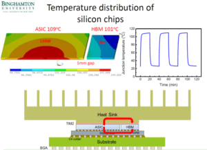
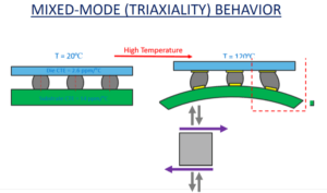
Park, in a very passionate and winning way, introduced the many electrical engineers in the audience to the world of thermal-mechanical effects that must be considered when selecting package materials as well as when co-designing die and package. He explained how different coefficients of thermal expansion (CTE) cause thermal-mechanical interactions between materials, resulting in warpage and possible cracks in interconnects during the manufacturing process, temperature cycling tests and/or actual operation. Park showed several case studies to explain how to simulate warpage, thermal conductivity and other effects package designers need to consider. He also emphasized that equal attention needs to be paid to the thermal-mechanical effects at the interface between the IC package and printed circuit board (PCBs). Figure 3 shows how a logic chip, that typically operates above 100°C junction temperature, can heat up an adjacent DRAM, force it to refresh more frequently, which results in significantly increased access times and possible reliability problems.
Test Solutions
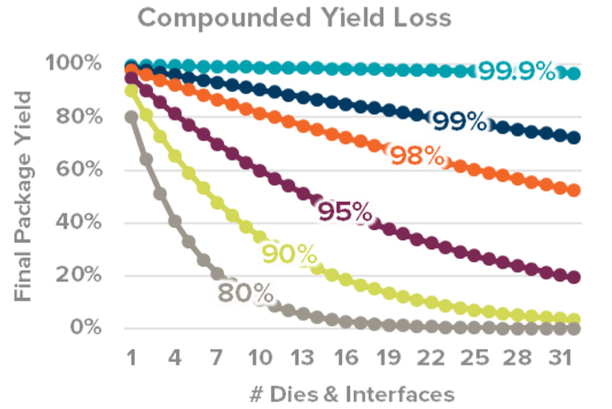
The third speaker, Timothy McMullen, Senior Director Strategic Marketing at FormFactor, addressed another important topic for improving the design and manufacturing cooperation for multi-die ICs: known good die (KGD). Because the yield of a final multi-die IC is the product of yields of individual dice, it’s very important that these dice (a.k.a. chiplets) are tested and function well (Figure 3.)
McMullen stated that economics speak against targeting KGD and suggested to consider probably good die (PGD) instead. He described the challenges of high-bandwidth memory (HBM) testing, with currently up to eight layers of DRAM dice, interconnected with 10,000s TSVs and vertical signal pipes at 40 by 60-micrometer pitch. Formfactor can test wafers at even smaller pitches, but the durability of such MEMS probe cards and probe tips decrease. McMullen is asking IC designers to plan more dedicated probe pads, add more scan chains and consider redundancy and self-test to help achieve very high yields, resulting in low unit cost.
The reliability of ICs and systems is becoming more important, as failures in medical, automotive, industrial and other applications can have very painful and costly consequences. Craig Hillman and his company “Design for Reliability (DfR) Solutions” has become so well known in this critical area, that ANSYS acquired them last May. Hillman explained the causes for common failure mechanisms like low-K dielectric cracking, solder joint fatigue, and micro-via separation. He showed failure analysis results, explained the underlying material physics and suggested countermeasures die and package designers can take to minimize reliability failures.

Feedback from the audience indicated that the Advanced Packaging session was clearly radically different, but useful to improve design experts’ understanding of IC materials and manufacturing challenges. It told IC design experts on how to reduce/avoid manufacturing challenges, production ramp-up delays, and excessive unit cost.
The Keynote
The highlight of EDPS is the dinner keynote on Thursday evening. This year Joseph Sawicki, Executive Vice President, IC EDA at Mentor, a Siemens Business, was our keynote speaker. His executive-level presentation focused on “The Impact of Artificial Intelligence (AI) on Semiconductors and EDA”.
By demonstrating the extremely rapid growth of data volumes, Sawicki established the need for AI to analyze all this data and derive actionable and beneficial conclusions from it.
Figure 5 shows how AI funding compares with investments in other hot technologies. After conveying this exciting fact, I have to admit that more than 80% of these funds were invested in China: Call to Action for U.S. executives!!!

Like several other speakers during EDPS, Sawicki emphasized that domain expertise is and will become even more important to serve high-growth markets and differentiate electronic system solutions. Higher-level synthesis tools, like Mentor’s Catapult, help to implement system-level requirements in silicon.
Summary:
EDPS 2019 was my 8th such symposium and I can proudly state: It was the most informative and useful one, I have contributed to. It’s great to see that IC packaging topics demand serious attention now and the need of working together, across the entire supply chain is recognized as mandatory. The number of attendees (about 60) and their very active participation in the presented topics was remarkable. Let’s hope that EDPS 2020 will further amplify the need for differentiated semiconductor solutions, AI, domain expertise and cooperation.
I hope to see you at EDPS 2020! Don’t forget to review – at no charge – all EDPS presentations here!
Thanks for reading….Herb


