
At this year’s International Wafer-level Packaging Conference, almost 1000 semiconductor experts from all parts of the supply chain gathered at the DoubleTree Hotel in San Jose from October 23 to 25. Among them were also several electronic design automation (EDA) experts who discussed how to streamline die-package-board co-design. They explained how EDA tools enable higher performance per Watt and contribute to reducing development time and unit cost, amplifying the main advantage this rapidly emerging wafer-level / panel-level packaging technology offers.
The conference started with Doug Yu’s excellent keynote about TSMC’s broad range of multi-die IC packaging solutions. Francoise’s blog will tell you more about this. My blog is focused on EDA-centric topics.
My EDA Perspective
Having contributed, with EDA tools, directly to the rapid market acceptance of the fabless and foundry business model and to the broad roll-out of several ASIC technologies, I have very high expectations for the contributions EDA tools and methodologies will be making for die-package-board co-design efforts and More-than-Moore technologies in general.
However, I am concerned, as outlined in my 2016 blog, that the “Great Divide between Semiconductor Design and Manufacturing” experts need to be bridged first before we can enjoy a highly productive and cost-effective supply chain for advanced packaging technologies.
Why do I now use “advanced packaging technologies” and no longer 2.5/3D ICs or SiP? Because the many single die ICs our customers will also develop can benefit equally from a smoothly operating design and manufacturing supply chain for advanced packaging technologies.
What’s Driving Data Integration?
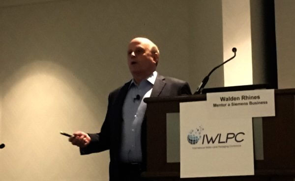
The point made by Wally Rhines, CEO Emeritus of Mentor, a Siemens Business, in his presentation titled “Discontinuities Drive Data Integration” makes the exact same point as my 2016 blog.
Rhines’ many years of management experience at a large semiconductor vendor (TI), and at a large EDA vendor (Mentor Graphics), combined with his excellent presentation skills made him a perfect fit to encourage the many manufacturing experts in the audience to work more closely with the much smaller EDA community. Only together can we serve mutual customers well and profitably.
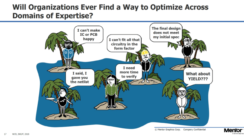
In the slide below (Figure 1) Rhines illustrated that thinking and operating in silos is nothing new. Cooperation has always been difficult across large corporations and is and will be even much more challenging across corporate boundaries in our highly fragmented advanced packaging supply chain.
Multi-die designs and advanced packaging technologies are important stepping stones to enable our IC industry’s transition from relatively low margin component suppliers to higher-value and more profitable (sub)system building-block providers. But how to win customers’ attention to encourage and follow this transition?
Listen up, System Architects!
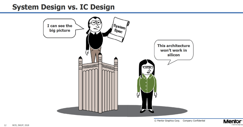
Rhines reminded the audience that the system architects, in coordination with C-level management, are the key drivers within our customers to adopt new technologies, like advanced packaging. Why? System architects don’t focus on the initial high cost of a new technology solution on the component-level. They recognize its potential for contributing to increasing their system’s value – e.g. by offering higher performance per Watt, smaller form-factors and cutting TOTAL system cost. Figure 2 shows an example of the tension between system architects and IC designers.
Demand is Up for Design and Verification Tools
At first, Rhines stated that designers only change if they must, then he mentioned the good news: In the last 18 months Mentor saw demand for die-package-board design and verification tools and flows taking off and invests accordingly.
As Mentor is working with key customers on deploying user-friendly die-package-board design flows, its EDA developers have to bridge the differences between traditional ways of designing die, versus packages and boards (Figure 3).

New tools also need to propagate design intent accurately to all design steps. For quick and easy change outs (ECOs) they must enable bidirectional data exchanges between design steps, to significantly simplify optimization of a design. All these capabilities enable designers to accomplish better performance and reduced unit cost much better and faster than with the traditional, spreadsheet-based methodologies.
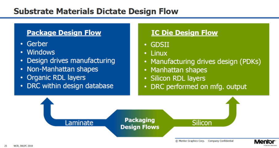
Figure 3, Courtesy of Dr. Rhines, CEO Emeritus of Mentor, a Siemens Business
Don’t Forget Pathfinding
In addition, Rhines emphasized the importance of good planning (a.k.a. Pathfinding) methodologies. They capture the characteristics of all functions integrated in an advanced package and allow system architects and designers to simulate/evaluate total design functionality as well as performance and power trade-offs. Such planning tools also quickly analyze die-to-die and die-to-package interactions, as well as discover design errors and inefficiencies early in the process where they can be fixed quickly and with much less effort than further down in the design/verification process.
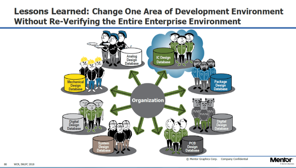
A multi-die advanced packaging solution comprises multiple dies and package components from different development teams, at the same or at different companies. Every one of these teams maintains their own database. It is also important to keep all these databases in sync, at least for the time a joint multi-die solution is being developed. If/when a change is introduced to one database, its impact to other databases and development teams needs to be analyzed and reacted to, so that costly surprises at the next development project can be avoided (Figure 4). EDA experts can assist the database managers to remain in sync, avoid surprises and project delays.
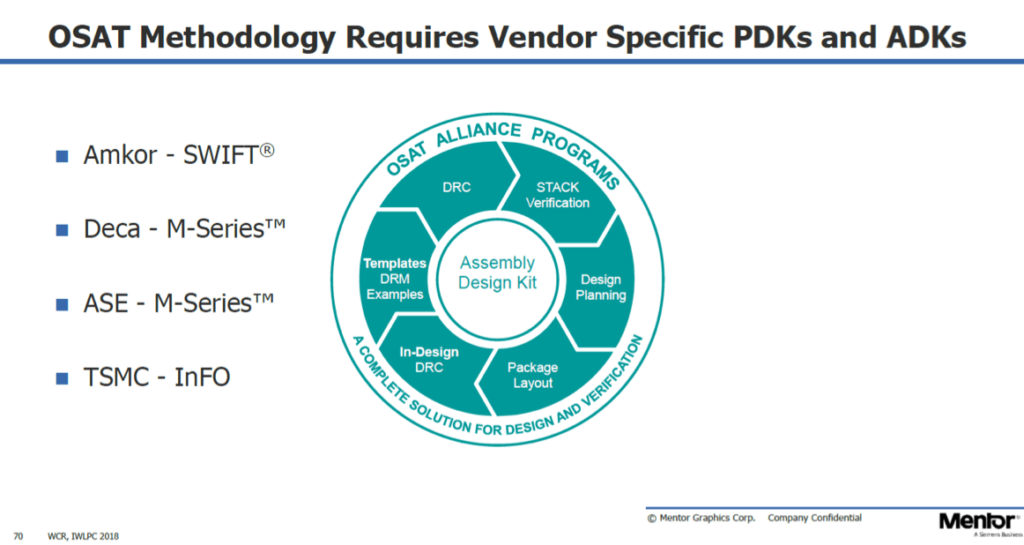
Rhines suggested we look at the bigger picture. He outlined the OSAT Alliance, Mentor’s way to enable advanced packaging manufacturers to work more efficiently, timely and cost-effectively, with their customers. Figure 5 lists several of Mentor’s development partners for wafer-level packaging solutions. It also shows important elements of an assembly design kit (ADK). It contains accurate and up-to-date data about the manufacturers’ equipment, manufacturing flow and materials capabilities, all essential inputs for the design tools. This allows designers to minimize margins and cost when optimizing a design. Learn more about Mentor’s approach to package design in their white paper series.
Learn from the Past
Allow me some personal comments to complement this informative keynote. 20+ years ago, TSMC and other foundries developed, together with their EDA partners, reference flows for die design and also created process design kits (PDKs), to convey wafer fabs’ capabilities. Together, these flows and PDKs have enabled the rapid emergence of the now very large and profitable fabless and foundry ecosystem.
Now we need to apply this proven concept to die-package-board CO-design flows and assembly design kits (ADKs), to enable economical design and manufacturing of system building blocks. Complemented by the right business arrangements, these flows and ADKs, as well as the emerging library of legacy building blocks, will develop into the core of a highly productive and cost-effective semiconductor ecosystem. System architects and IC designers at our customers will be able to rely on this library of higher-level building blocks when creating, customizing or updating system solutions.
Considering that wafer foundries and their EDA partners frequently update and thoroughly verify reference flows and PDKs and have served the fabless & foundry industry well for the last 20+ years, I am optimistic that we’ll not only build but also maintain this new, considerably more complex “designers & manufacturers” ecosystem well.
Please note that I am not able to give a schedule for an industry-wide roll-out of this ecosystem. At this time, I can only tell you that TSMC will again be the trendsetter. ~ Herb
Keith Felton from Mentor, a Siemens Business, and Bill Acito from Cadence Design Systems, gave in-depth technical presentations in Session 3 and showed how their respective die-package-board design tools and flows contribute to creating cost-effective advanced packaging solutions. My next IWLPC blog will focus on their messages.


