
Recently, I read a paper published in the 2017 IMAPS Device Packaging Conference proceedings, titled “Cost Comparison of Fan-out Wafer Level Packaging and Flip Chip Packaging,” written by Amy Lujan, of Savansys. Lujan did a very good analysis on the cost comparison of fan-out wafer-level packaging (FOWLP) with chip-first and die face-down and flip chip (FC) packaging, according to an activity-based cost (ABC) modeling. Emphasis was placed on the cost comparison to determine which design features drive a design to be packaged more cost-effectively as an FC package, and which design features result in a lower cost FOWLP. A wide range of chip/package sizes has been considered [1].
The purpose of this post based on Lujan’s findings [1] is to focus only on the potential “real” application ranges of FOWLP, i.e., package/chip ratio. The present conclusions are shown at the bottom of all the figures, except Figure 1, from [1].
Analyses
Figure 1 shows the process of the FC packaging and FOWLP.
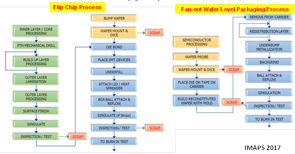
Figure 2 shows the processing cost comparison of FC and FOWLP by varying package sizes and considering two chip sizes (5mmx5mm and 3mmx3mm). For both chip sizes, in the application range of FOWLP (package/chip ratio = 3.24 and 4, respectively), the processing cost of FOWLP is lower than that of FC packaging.
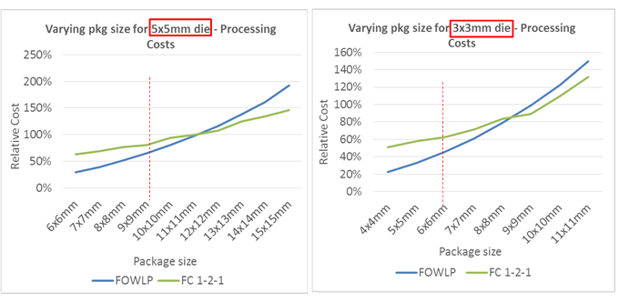
Figure 3 shows the processing cost comparison of FC and FOWLP by varying chip sizes and considering one package size (13mmx13mm). It can be seen that, in the application range of FOWLP (package/chip ratio = 2.64), the processing cost of FOWLP is lower than that of a FC package.
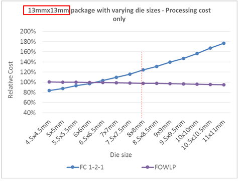
Figure 4 shows the processing + die cost comparison of FC and FOWLP by varying chip sizes and considering two die costs ($1 and $2). The package size = 13mmx13mm. It can be seen that, in the application range of FOWLP (package/chip ratio = 2.64), the processing cost (with the die cost included) of FOWLP is lower than that of FC package.
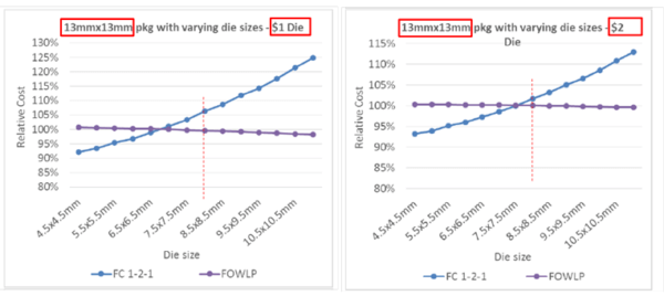
Figure 5 shows the processing cost + yield comparison of FC and FOWLP by varying package sizes and considering two die costs ($1 and $2). The chip size = 3mmx3mm. It can be seen that, in the application range of FOWLP (package/chip ratio = 2.8), even with all the yield loss considered for FOWLP, the processing cost (with the die cost included) of FOWLP is cheaper than that of FC package. For the definition of processing yield, please read [1].
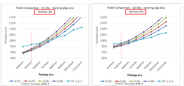
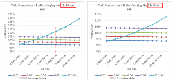
Figure 6 shows the processing cost + yield comparison of FC and FOWLP by varying chip sizes and considering two die costs ($1 and $2). The package size = 13mmx13mm. It can be seen that, in the application range of FOWLP (package/chip ratio = 2.34), even with all the yield loss considered for FOWLP, the processing cost (with the die cost included) of FOWLP is lower than that of FC package.

Summary
Some important results are summarized as follows:
- Based on Lujan’s ABC modeling and findings [1], and focus on the application ranges of FOWLP, i.e., package/chip ratio, some useful conclusions have been obtained.
- For all the cases considered, the cost of FOWLP is lower than that of FC packaging.
Reference
[1] Lujan, A. P., “Cost Comparison of Fan-out Wafer Level Packaging and Flip Chip Packaging”, IMAPS 2017, pp. 1-5.
For other reading on this topic, see the Amy Lujan’s 3D InCites post, also based on her paper.