

![]()
Three-dimensional Integrated circuits (3DIC) are generating increased interest as a way to increase speed and density while reducing power and form factor. System level integration in Package (SiP) has joined “System on Chip (SoC)” as one of the primary mechanisms to drive the electronics industry. Quotes such as “Smartphones and Tablets will increasingly owe their prowess to better chip packaging” [Apte11] are now common, and consortia such as the International Technology Roadmap for Semiconductors [ITRS09], SEMI [3DS-IC], Si2 [Open3D], JEDEC [3D-ICs] have all established committees or focus areas on 3DIC. The challenges to develop 3DIC technologies, however, are formidable, encompassing supply chains, manufacturing, standardization, and design technology.
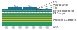
This paper focuses on a fundamental aspect of design technology for 3DICs: Understanding the electromagnetic behavior of 3D structures and how to model them in practice. It examines novel electromagnetic modeling aspects of 3DICs, in particular, the use of silicon substrates such as silicon interposer, redistribution layer (RDL) and Through Silicon Via (TSV). It shows how to model electromagnetic properties of silicon substrates, RDL and TSV, how to capture the physical effects in a full 3D solver, and how to incorporate these models into electromagnetic simulation tools. The paper concludes with some examples that illustrate the techniques we have developed.


