

Demand for EVG wafer bonding solutions driven by accelerated production ramp in advanced packaging, advanced MEMS devices, and CMOS image sensors

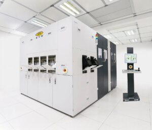
FLORIAN, Austria, May 16, 2017—EV Group (EVG), a leading supplier of wafer bonding and lithography equipment for the MEMS, nanotechnology and semiconductor markets, today announced that it has achieved an industry milestone with more than 1100 EVG wafer bonding chambers installed at customer facilities worldwide to date. This milestone cements EVG’s technology and market leadership in wafer bonding, which is an enabling process for volume manufacturing of semiconductor advanced packaging, MEMS, CMOS image sensors, and radio frequency (RF) devices. The EVG®500, EVG®850, GEMINI® and ComBond® series of wafer bonding solutions, in particular, are seeing strong demand due to their industry-leading performance and cross-platform compatibility, which allows customers to more easily ramp up their R&D processes to high-volume manufacturing.
“For our high-volume customers, it is essential that they have ready access to industry-proven, cost-effective and high-yielding process solutions. EV Group has closely collaborated with customers and partners for nearly three decades to innovate wafer bonding technology, which has led to the establishment of our technology as the de-facto industry standard for high-volume manufacturing,” stated Hermann Waltl, executive sales and customer support director at EV Group. “Our product offerings span the entire manufacturing chain from R&D and small-scale production environments to full-scale, high-volume production. This enables us to support our customers throughout as they transform new ideas into real-world products.”
EVG’s wafer bonding solutions for adhesive and fusion/hybrid bonding, metal bonding (such as solder and eutectic), and high-vacuum encapsulation undergo continuous innovation in a variety of critical areas, including temperature and process uniformity, vacuum control, wafer alignment and ease of use to ensure a high-yielding and high-throughput bonding process. Manual and semi-automated wafer bonders are fully compatible with EVG production bonding systems, which shortens the development time for customers to bring new innovative devices to market.
For adhesive, solder and eutectic bonding, the EVG500 series of semi-automated wafer bonders and GEMINI series of fully automated wafer bonders support non-hermetic, cost-efficient encapsulation of CMOS image sensors, surface acoustic wave (SAW) filters for wireless RF chips, and other devices for mobile phones and other high-volume consumer applications. Additionally, tool configurations can be tailored to more demanding bond processes such as hermetic encapsulation for MEMS devices.
For high-vacuum encapsulation bonding, the new EVG ComBond automated high-vacuum wafer bonder provides ultra-high vacuum encapsulation (10-8 mbar) needed for next-generation MEMS devices, such as gyroscopes, microbolometers, and advanced sensors used in autonomous cars, virtual reality headsets, and other applications.

For fusion bonding, the EVG850LT and the GEMINI FB automated fusion bonders enable manufacturing of high-accuracy optical devices, image sensors, and engineered substrates such as silicon-on-insulator (SOI), silicon carbide (SiC) and gallium nitride (GaN) for RF, power and other high-speed/high-efficiency devices.
Added Waltl, “EVG is continuously improving our process solutions in order to address wider market applications and more stringent industry requirements. This has paid off for our customers, which in turn has enabled us to maintain our leadership position in the wafer bonding market. Every four seconds, a wafer is bonded with an EVG system. We are proud to bring our expertise gained from this far-reaching installed base to our customers around the world.”
More information on EVG’s wafer bonding solutions can be found at: http://www.evgroup.com/en/products/bonding/waferbonding/.


