

Latest Posts
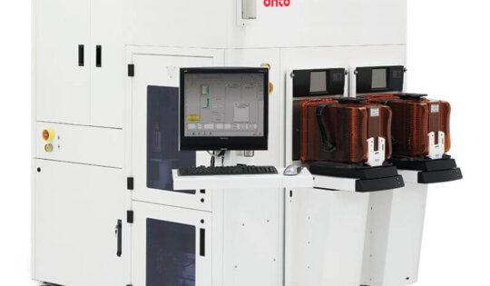
Onto Innovation’s Dragonfly® Inspection Platform Projecting Record Annual Growth in 2021
Dragonfly system growth accelerated by tier 1 customer adoption WILMINGTON, Mass.–(BUSINESS WIRE)– Onto Innovation Inc. (NYSE: ONTO) (“Onto Innovation”, “Onto”,...
EV Group Expands Production Capacity at Corporate Headquarters in Austria
EV Group (EVG), a leading supplier of wafer bonding and lithography equipment for the MEMS, nanotechnology and semiconductor markets, today...
EV Group Achieves Industry Milestone With Over 1100 Wafer Bonding Chambers Installed Worldwide
Demand for EVG wafer bonding solutions driven by accelerated production ramp in advanced packaging, advanced MEMS devices, and CMOS image...
Hugo Pristauz Drops the F-bomb at 3D ASIP 2016, You Won’t Believe What Happens Next!
Sorry everybody, but I couldn’t resist this Buzzfeed-esque title, because Besi’s Hugo Pristauz’ unprecedented use of “colorful” language to illustrate...
Combining Technology Platforms and Integrating Complex Materials for New Applications
Heterogeneous integration is in many ways different from other research technology platforms. For one thing, the technology is mostly driven...
In Conversation with Yann Guillou About the SEMI European MEMS Summit 2015
Yann Guillou, Membership & Business Development, SEMI Europe, talked with 3D InCites / 3D+ about the upcoming European MEMS Summit...
Diverse Technology Selections Served at CS MANTECH 2015
What were all these silicon people doing at a compound semiconductor conference? CS MANTECH 2015 was the 30th anniversary version...
The Future of Image Sensors is Chip Stacking
CMOS image sensors (CIS) have often been heralded as the first 3D devices in volume manufacturing. However, this is not really...
SPTS Technologies’ Sigma fxP PVD System Selected by HuaTian Technologies for 300mm Flip Chip Bumping and CMOS Image Sensor Applications
One of China’s Leading Semiconductor Packaging Providers Chooses SPTS PVD Solution for new 300mm Expansion Newport, United Kingdom, 8 July, 2014 –...
SPTS Technologies’ Silicon Etch Tool Chosen for 300mm CMOS Image Sensor Applicatons
Move to 300mm Strengthens Customer’s Position in the Rapidly Growing CMOS Image Sensor Market Newport, United Kingdom, 29 May, 2014...
3D Wafer Level Packaging: Outlook for 2014
In 2013, SPTS equipment sales into the advanced packaging market grew by 75%. Some of this was due to a...
EV Group: Never a Dull Moment
This is part of a series of short interviews, based on face-to-face meetings at SEMICON West 2013. Sitting down with... EV Group Pushes the Limits on 3D-IC Manufacturing for Next-Generation CMOS Image Sensory
Enhanced wafer alignment metrology capability coupled with market-leading GEMINI® FB system creates closed-loop fusion wafer bonding solution to enable high-density...Ziptronix Signs Licensing Agreement with Sony
Ziptronix, Inc. has signed a licensing agreement with Sony Corporation for the use of Ziptronix’s patents regarding oxide bonding technology...Wafer-Level Microlens Molding Process From EV Group Extends Manufacturing Roadmap for CMOS Image Sensors
EV Group (EVG), supplier of wafer bonding and lithography equipment for the MEMS, nanotechnology and semiconductor markets, announced that it...SPP/SPTS ships 300mm DRIE tool to CEA-LETI
SPP Process Technology Systems (SPTS) and its parent company