
More and more applications are calling for miniaturized electronics to integrate high-performance devices in a limited volume. 3D technology is being driven by the consumer markets as smartphones, tablets and many handheld devices require advanced features in light and thin products. Currently, those requirements are being fulfilled by fan-in or package on package (PoP) technologies, but real 3D low-profile components are being introduced for specific applications. Through silicon via (TSV) is the main driving technology, even though drawbacks are still slowing down its introduction such as:
- Highly specific designs that make multi-sourcing difficult
- Final 3D component yield decreased drastically as wafer level yield is good enough
- TSV yield
- TSV cost
Alternative technologies are being developed to get through those issues mainly for highly heterogeneous systems-in-package (SiPs) for which multi-sourcing is a must. 3D PLUS proposes a unique solution that overcomes many TSV issues:
- High yield due to stacking only known-good rebuilt wafers
- Using standard wafers without TSVs ensures compatibility for multi-sourcing
- Very small form factor; several dies per level are possible
- The thickness of each layer: 250 to 100μm (10 levels/mm).
- Technology can be applied to 300 or 200 mm wafer or in panel form.
Wafer level package manufacturers include a double-faced redistribution layer (RDL) in their roadmaps as the first step for 3D integration with PoP solutions. 3D PLUS is a step ahead of this with stacking several rebuilt wafers using its patented bus metal interconnect.
Two years ago, first results were shown with FPGA 3D module and leadless pacemaker [1]. In this article, we present two new applications for implantable applications.
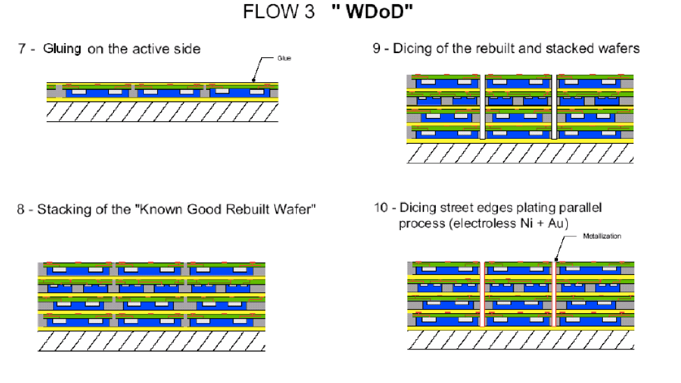
Wire-free die-on-die (WDoD™), developed by 3D PLUS, is an innovative 3D technology that involves stacking known-good rebuilt wafers with only known good dies (KGD). Based on stacking 2D fan-out wafer level packaging (FOWLP) and printed circuit board (PCBs), interconnections are performed with metal bus metal patterned with a laser. First, rebuilt wafers are manufactured using eWLB and reconstituted chip package (RCP) technology as follows (figure 1):
- Pick, flip, and place KGD from the die wafer to a 200mm or 300mm carrier wafer on thermal release tape.
- Compression molding is performed using epoxy resin with silica fillers.
- Known good rebuilt wafers go through a grinding step to decrease total thickness to 250μm or less.
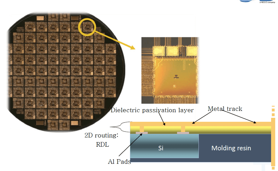
- Fan-out built-up with redistribution layer process (Figure 2).
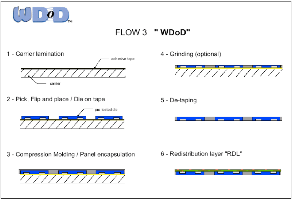
- First, known-good rebuilt wafer is glued, followed by sequential stacking and gluing.
- Rebuilt and stacked wafers are diced.
- Dicing of rebuilt and stacked wafers.
- Dicing streets are plated using an electroless process.
- All these steps are performed collectively at the wafer level.
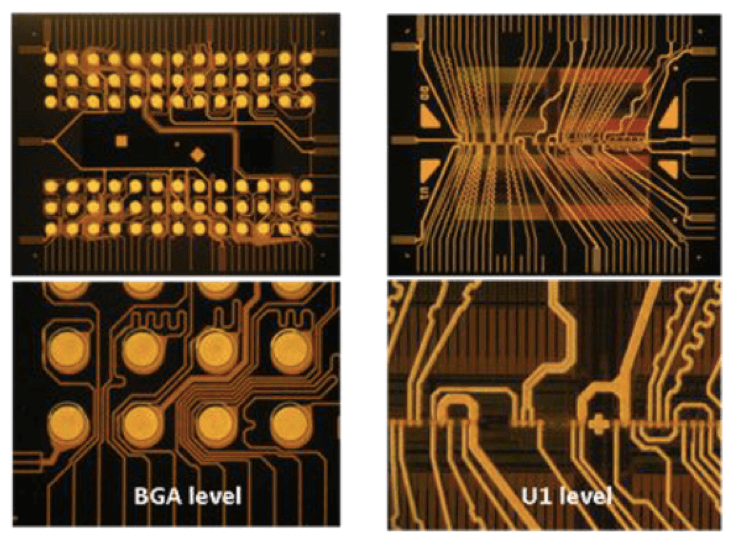
- The final laser patterning on the plated edges of each module is the final step before the electrical test. (Figure 3)
In partnership with LivaNova a medical device innovator, 3D PLUS conducted a feasibility study that involved designing and manufacturing two different electronic modules for implantable products.
This first application, developed for a French PIA project (INTENSE), targeted neurostimulation for severe conditions, particularly heart failure. One of the challenges was to reach a very low-volume for this device. Standard die assembly processes (chip-on-board, die stacking) currently used by LivaNova did not allow them to reach this objective. As the bill of materials (BOM) only contained dies (ASICs and PICS capacitors) WDoD was a good candidate. The design was developed in collaboration with LivaNova and NANIUM to align with the latter’s industrial design rules.
Approximately 30 modules were manufactured by 3D PLUS, on which continuity tests were successfully performance. Functional tests are in progress at LivaNova. In parallel, we have launched with success JEDEC MSL 3 qualification flow as this module must be assembled on a PCB as a standard BGA component. This product is a good example of what can be produced with WDoD technology.
The second example is a leadless pacemaker:
More than 1 000 000 pacemakers and more than 200 000 defibrillators are implanted in the world each year. All these devices need 3D heterogeneous integration to reduce the size of the electronics. Leadless pacemakers are expected to be revolutionary to the cardiac rhythm management (CRM) industry, especially in the US and EU by eliminating the need for lead replacement. The state of the art for the volume of a subcutaneous pacemaker is 8 cm3 and for a leadless pacemaker is 1 cm3. MANpower FP7 NMP was launched in 2013 to develop a new leadless pacemaker system to be inserted into the cylindrical capsule.
3D PLUS was challenged to develop a new 3D module using its WDoD technology. The BOM included many surface mount device (SMD) components and only one ASIC die. The strategy would have been to stack one fan-out level with the die and other printed circuit board (PCB) levels with SMD components. But due to a tight time schedule, we had to find another solution than Fan-Out for the level with the ASIC. 3D PLUS developed and patented a new process named Flow3.5 based on the concept of a 2D level with straight and flat wire bonds interconnecting the ASIC die with a sacrificial PCB.
As such, we know that WDOD can be applied to:
- Flat wire bonding
- over molding
- grinding
- stacking
Compared with FOWLP levels, the total thickness of this level can be in the range of 500μm, which is less challenging than the thickness of FOWLP levels (250μm). But prototyping lead time can be reduced significantly, therefore Flow3.5 can be a good option when no RDL is necessary. We decided to build the level with dies using Flow 3.5 technology. The 3D module finally fits within the available cylinder volume of 6mm diameter and a maximum length of 6mm. All the SMD components were placed on two class 11 PCBs. Some of them were on external sides. Comparison with the alternative flex-folded integration of the same Bill of Material shows that the 3D PLUS module length = 65% of flex-folded solution length.
WD DoD technology versus embedded die technology

There several differences between embedded die in the PCB versus WDoDs. Embedded ICs present some distinctive characteristics such as:
- The ability to use only small die (maximum dimensions 5 x 5 mm)
- Die pads must be plated with copper
- Die drift during PCB curing is more important than with fan-out technology.
- If several dice are embedded, the accuracy of their location could be critical (one of the advantages of fan-out is the use of an isotropic epoxy resin with silica filler)
- A full system with different die and passive components will have a large area because it is 2D technique.
Conclusions
The interest of WDoD, with or without FOWLP (Flow 3.5) has been shown in 2 examples of implantable applications where competitor technologies like chip-on-chip, flex folded or hybrid technology would not have permitted the form-factors expected
WDoD or Flow3.5 allows 3D stacking of heterogeneous BoM with mature 2D technologies (PCB, Fan-Out). BGA modules or modules with specific connections can be obtained with this technology.
Acknowledgements
This work has been partly supported by the European Commission Framework Program 7 within the project MANPOWER (Project-no FP7- NMP-2013-SMALL-7 604360) and the French PIA project INTENSE
We want to thank NANIUM for their expertise for the design and manufacturing of 2D Fan-Out levels.
References
[1] P. Couderc “SiPs in the medical domain and in the defense and industrial domain produced with WDoDTM technology”, Device Packaging Conference 2015, October, Scottsdale, USA
[2] J. Noiray, C. Val, P. Couderc, T. Ferrara, “Stacking of Known Good rebuild wafers for high-performance memory application to high-speed DDR3”, Minapad 2012, April 25-26, Grenoble, France
[3] P. Couderc, J. Noiray, C. Val, “Stacking of Known Good rebuild wafers for high-performance memory application to high speed and SiP”, IMAPS 2013, October, Orlando, USA
This paper was first presented at the IMAPS Device Packaging Conference 2017. The presentation can be downloaded here.

Comments are closed.