Semiconductor device fabrication and packaging is rife with acronyms, and by my estimate, the Top 3 trafficked by speakers at the recent IMAPS Device Packaging Conference were the acronyms FOWLP, FOPLP, and MEMS.
That would be fan-out wafer level packaging, fan-out panel level packaging, and microelectromechanical systems, respectively.
It wasn’t that IMAPS was a MEMS packaging conference in the strictest sense, but, with heterogeneous integration being one of the most important ways electronic system performance will continue to advance in the face of only-a-few-can-afford-to-play-single-digit-nanometer CMOS, and with MEMS component content almost a given when speaking of internet of things (IoT) or industrial internet of things (IIoT) applications, much less when speaking of smartphones or automotive, we heard lots about MEMS packaging at IMAPS.
 My radio picks up MEMS stations transmitting even the weakest of broadcast signals, but in Scottsdale, AZ, this month it’s as if every station on the air, meaning almost every talk, included a loud and clear MEMS call sign.
A remarkable confirmation of MEMS ascendant in this, the Year of the Rooster.
One only need consider the keynote talks given at IMAPS Device Packaging to get a sense of what I mean.
For Ron Huemoeller, Amkor, in “Heterogeneous Integration: Packaging the Future,” the mobility segment, the consumer / IoT segment, the automotive segment, and the high-performance computing segment are the strong drivers pushing packaging technology forward, and among those segments three of the four (mobility, IoT, automotive) ride in on MEMS and sensors. So we’d best figure out now how to address multi-die heterogeneously integrated System-in-Package technology, with MEMS, for not just high-end uses, but also for mid-range, and maybe even entry-level, markets in mobility, IoT, and automotive – whatever the best use case is. We should be enabling “more die content in a smaller space, working more efficiently,” as the alternative to the dark silicon – diminishing returns that is advanced SoC.
 “Innovations of the hippest,” according to Lionel Rudant, CEA-Leti, are arriving in artificial intelligence (AI), robotics, and in the merger of the cyber and physical worlds that is coming in the new forms (think augmented reality (AR) of digital user experience, with the mantra to “deploy smart systems into small objects.” And they will be chatty small objects, looking to share data in order to announce status, announce intentions, or to synchronize trajectories in the cases where the smart small objects themselves are in motion, for example as autonomous vehicles during rush hour on the 101.
This hip future rests on 5G network deployment, scheduled for commercial rollout at the Tokyo Olympics in 2020; 5G network deployment depends on successfully integrating large numbers of RF filters (a MEMS application), RF switches (could be MEMS – indulge me!), and multi-element beam forming antennae as an important triumvirate of elements for the 5G transceivers. MEMS packaging options are many.
![[err-ad-fallback-title]](http://www.3dincites.com/wp-content/plugins/a3-lazy-load/assets/images/lazy_placeholder.gif)
 I think Jim Walker (was Gartner, now independent at World Level Packaging Concepts) has it about right when he says “heterogeneous integration continues Moore’s Law, consolidation must occur in the SATS/OSAT market, resulting in its stratification, and advanced packaging will enable complex systems at affordable costs.” I also like it when he calls out smart home, smart city, and connected car as driving a 9.6% CAGR for the non-optical sensor / MEMS device market through CY2020.
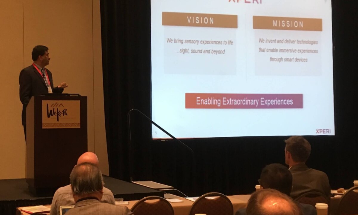
And this one is pretty much a gimme: Sitaram Arkalgud, XPERI, on “Trends in MEMS and Sensor Integration.”
And so is this one: Markus Leitgeb, AT&S, a leader in high-end PCBs for high-end applications, notes that the AT&S technology roadmap for printed circuit boards includes in development the functional integration of sensors & MEMS components. system-in-board (SiB) may just be what follows system-in-package. According to Markus, “Let’s make PCB great again.”
 Let me know if it’s just me, but when four of the four IMAPS DPC keynote speakers, along with a fifth keynote from the IMAPS Global Business Council program, all feature MEMS content in their device packaging talks, then I say MEMS has surely arrived, and that 2017 is the year of MEMS ascendant.
From Santa Clara, CA, thanks for reading. ~PFW