
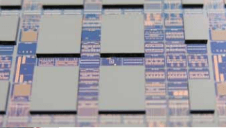
 Multi-project wafer (MPW) programs have long been considered an economical way to integrate different IC designs from various teams to produce IC design prototypes and low volumes. Because IC fabrication costs are extremely high, it makes sense to share mask and wafer resources in this way. MPWs were historically used for 2D designs, but in 2009, Tezzaron Semiconductor launched an MPW for DARPA to develop 3D logic devices that would then be integrated with a Tezzaron DRAM to create a hybrid memory/logic 3D-IC. This was the first MPW to serve 3D integration technologies.
Earlier this year, French institutes IRT Nanoelec and CMP (Circuits Multi-Projets) teamed up to offer an MPW for 3D post-process technologies – a reported industry first as the Tezzaron MPW projects have focused on front-end TSV manufacturing processes to interconnect logic and DRAM. I caught up with Kholdoun Torki, technical director of CMP to learn more about this program, and what it means for furthering the 3D IC cause.
The Back Story
Established in 1981, CMP is a service organization that provides MPW programs for prototype and low-volume IC and MEMS production. According to Torki, CMP customers include universities, research laboratories and small to medium fabless companies. In fact, in 2011, CMP worked with Tezzaron on a 3D IC project at 130nm. Torki explained they collected designs and provided participants with access to the design kits, and verified layouts.
Typically CMP partners with ams and ST Microelectronics to procure silicon. To date, 6,700 projects have been prototyped for more than 1000 institutions from 70 countries. This is the first MPW that focuses on 3D assembly processes.
IRT Nanoelec, headed by CEA-Leti, conducts R&D to drive new product development and applications, such as the Internet of Things, in information and communication technologies. IRT Nanoelec provides early insight into how emerging technologies such as 3D integration and silicon photonics will affect integrated circuits. IRT also runs a technology transfer program to bring the technologies developed there market. IRT Nanoelec’s 3D technology toolbox contains through silicon vias (TSV,
via last), fine-pitch vertical interconnects (micro pillar with solder) and specific finishing for 3D integration like under-bump metallurgy (UBM).
MPW for Post-process 3D Integration
Up until now, the missing piece for 3D IC MPW was 3D assembly processes such as via-last TSVs, microbumps, Cu pillars, “Now we can select a subset of what Leti is offering (through it’s Open3D consortium) and share the cost between different users to have an affordable cost for chip-on-wafer packaging,” explained Torki. These 3D modules will enable a wide panel of new, full 3D architectures, like multiple-die stacking with flip-chip, side-by-side heterogeneous integration, and 3D partitioning of different CMOS dies issued from CMP runs. CMP’s goal is to validate concepts for new designs. “We’re not addressing products, we’re addressing the feasibility of a challenging device. After we know, we won’t be providing the mass production, “ he said.

What this collaborative effort is providing falls along the lines of what some members of the design community has been clamoring for –an assembly design kit for interposers and 3D assembly. As a service provider, Torki explained that CMP will identify the process to give access to users. Leti offers an affordable, stable process, he explained. The plan is for CMP to subcontract the assembly to Leti. “We’ve added on a module for 3D in the design kit to address bumps for TSVs,” he said. Working with Mentor Callibre, they currently verify two tiers. “In a few years, we will have tools that verify the entire assembly,” he noted.
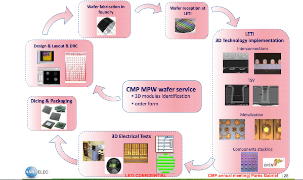
These 3D post-process technologies require very limited re-design of existing chips, and will be initially used for specific CMOS nodes available at CMP. They may be extended in the future, depending on demand. CMP is responsible for supporting, checking and compiling the customer’s requests, while IRT Nanoelec will manage the 3D post-processing (Figure 1).
According to Torki, the collaboration between CMP and Nanoelec IRT has already successfully completed one run with 20 projects. He invites companies and universities around the world to submit their designs for the MPW. For small to medium size companies interested in getting a toe-hold in the 3D space, this may the most cost effective way to do it. ~ F.v.T.


