


Interconnectology returned as a topic of discussion to the 2014 BiTS Workshop through a keynote discussion delivered by Invensas’ president, Simon McElrea. His talk, aptly titled “Interconnectology: the Road to 3D” addressed the need not only for innovations in interconnect technology that focus less on silicon innovation and more on advanced packaging; but equally about the interconnectology of people to communicate across the supply chain to tackle the remaining chokepoints for adoption of 2.5D and 3D IC technologies. “Today, technologies are not just lifted off a shelf. The products are designed with everything in mind, and that includes packaging and test,” he noted.
To me, McElrea’s most compelling point was the idea that the organizations that ultimately take 2.5D and 3D IC to commercialization may not be the traditional semiconductor players, (foundries, OSATS, IDMs, etc.) but rather the end-product owners who are weary of waiting for solutions to their high-performance, low-power needs and will take matters into their own hands; companies like Apple, Google, Microsoft, Facebook and Amazon.
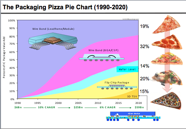
There is a considerable value proposition that goes with the advanced processes required for wafer level and 3D packaging. Using a pizza analogy, McElrea explained that while legacy and lower I/O packages still dominate the (pizza) pie chart, the more complex the device, the higher its value (cheese pizza vs. the “house special”). Although the die area per package technology (line loading) is hardly changing, the return on the advanced nodes, flip-chip, stacked-CSP, WLP, is growing at 20% CAGR, he said (Figure 1). McElrea predicted that newer companies will be the ones to exploit high value packaging, leaving older companies to the simpler, legacy technologies. “The adoption curve (of 2.5D and 3D IC) depends on which players the supply chain will permit to own the new value added elements,” he said. “History says it’s the model that provides the greatest sourcing feasibility to the end-product owners.”
At the end of the day, the answer to the question “who pays?” comes down to who needs it the most, noted McElrea. TSV processing requires high cost equipment sets traditionally seen in the wafer fab including those needed for lithography, etch, clean and deposition processes, as well as high-cost, low throughput bonders. CapEx requirements could segment the OSATS companies and reduce competition in this market, noted McElrea.
“Being in heart of Silicon Valley, we’ve seen a revolution from companies like Google, and Apple, and Microsoft/Nokia, who are investing in semiconductor packaging because they need to.” He went on to explain that obtaining the silicon – logic, memory, RF and sensor devices – is not the issue. The need for these companies comes from trying to integrate various functionality into their products; smaller handheld and wearable devices (Figure 2). “If the supply chain doesn’t come forward with all the investment that’s needed, it wouldn’t be too surprising – and it wouldn’t be the first time – if the investment came from the top level; the Apples, the Googles, the Samsungs,” he noted, citing Apple’s push to develop NAND Flash to fulfill the non-volatile memory requirements of its early generation iPod nano.


Another key take-away from McElrea’s talk was the lessons learned from package-on-package (PoP). “PoP is a 3D solution with a beautiful business model, because it provides a way of separating the memory supplier from the logic supplier,” he said, noting that PoP is the dominant source of revenue being made by top OSATS.
So if PoP does everything we need, why the shift to 3D IC at all? “It’s mostly about cost. And PoP doesn’t do everything we need,” says McElrea. Rather, he says we have to emulate the PoP business model to the best of our ability in 2.5D and 3D IC. “These products are clearly technically better with greater bandwidth, lower power, and smaller size, but if we don’t deal with issues of supply chain liability, the ability to test and determine yields, and for companies to work together in the model, its just going to be problematic and time consuming to get to high volume.” He recommends taking elements from PoP and applying to 2.5D and 3D IC.
The good news is, one way or the other, we’re closer than ever to making this happen. While only a handful of companies have taken the leap to production, McElrea says another telltale sign that we are on the brink of adoption is the increase in CapEx beyond R&D in the manufacturing environment.
Will the shift to 3D ICs ultimately require a paradigm shift? McElrea sure seems to think so. “The need is here,” he says. “If the industry won’t make it happen, end product owners will make it happen.” As for me, I like my pizza loaded, but hold the anchovies please. ~ F.v.T.


