
The transition to 3D NAND Flash seems to be imminent with projections of it being half the total NAND Flash market by 2016. That means tens of billions of dollars within 3 years.
V-NAND is Samsung’s version. Their first publication describing this architecture was released in 2009 and was called “TCAT” or “Terabit Cell Array Transistor”.
Toshiba too has been working on a similar technology which they call “BiCS” or “Bit Cost Scalable” and variants thereof and was actually first to publish back in 2007.
Both approaches are broadly similar in two key features which mark a sea-change in how NAND Flash is made.
First, both rely on a “charge trap flash” (CTF) approach to store electric charge. This is an insulating film, usually based on a silicon nitride material, where charge can be placed. This is in contrast to standard NAND Flash, which uses a “floating gate” approach where an isolated conductor stores charge. Both approaches have a long history going back to the late 1960’s. Ironically, the charge trap approach is a year or two older.
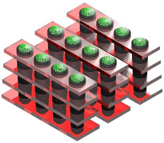
Second, both approaches have a vertical channel. That is, electrical conduction through the NAND Flash string is perpendicular to the NAND chip’s surface as opposed to horizontal in the standard NAND. To help picture this, Figure 1 shows a generic vertical channel approach that could be both V-NAND or BiCS. The channels are vertical green cylinders and the gates are horizontal red bars.
The whole point of this kind of structure is to reach large single chip memory capacities at lower cost than any other approach whether it be 3D or regular NAND. The approach relies on deposition of an alternating stack of two types of material, which is then etched through after a couple of relatively simple photolithography steps that define holes and slits at the top of this stack. These then need to be filled with various materials such as the memory dielectrics that eventually need to trap charge, and amorphous silicon that forms the vertical channels. The conventional wisdom is that, compared with 3D approaches that would use photolithography steps on each device layer, this vertical channel approach would have far less expensive photolithography steps and therefore be much cheaper. Figure 1 shows the result.
So far so good then? Well, not quite. And this is where it gets interesting especially with tens of billions of dollars at stake.
First, take those holes and slits. These are small at the top but extremely deep and they need to be filled with materials that stick to the sidewalls in a precise fashion that is identical from top to bottom. This turns out to need “game-changing” fab equipment that the equipment vendors have jumped aboard to try to develop. Needless to say, it’s not a use-existing-fab-tools story anymore.
Second, any semiconductor memory technology needs a path towards higher capacity memory chips once the first one has been made. In this particular 3D approach, this could be a lateral shrink combined with more stacked cells. It turns out that the lateral shrinking is as good as exhausted since it would impede the formation of the memory dielectrics and channels. The only way would be to stack more cells, which then lengthens the channel (that green cylindrical tube in Figure 1). This results in ever-decreasing electrical currents out of the memory that get extremely difficult to sense. For those really interested, this is called the “vanishing worst case string current problem”.
Third and most important, let’s take a look at the real cost. Remember that low cost is the justification for this over other possible 3D Flash approaches. Since my company, Schiltron Corporation, is associated with these other approaches, any criticism from me on cost could be regarded as highly self-serving. Therefore, I wrote a peer-reviewed paper which has been accepted for publication in November’s edition of the IEEE Transactions on Semiconductor Manufacturing. An early access version can be downloaded free of charge from the IEEE website. (If you read this blog in November 2013 or afterwards, the open access published article can be found by starting at the IEEE Transactions on Semiconductor Manufacturing website and navigating to November’s edition of the journal.)

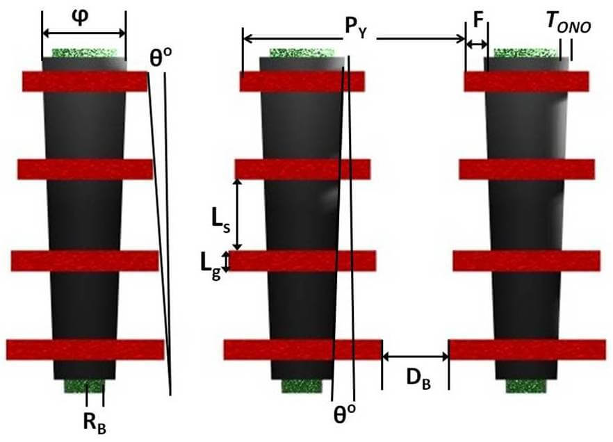 It turns out that there are two key structural parameters that define the total cost of this vertical channel approach such as Samsung’s V-NAND. Figure 2 shows several parameters in a cross section through the structure of figure 2. The most important parameter is theta, the taper angle from the vertical of the hole and slit. The second most important is the sum of Lg and Ls which are the memory cell’s gate length and space.
The conclusion from this study is quite illuminating. Let me quote it verbatim from the paper:
“A general principle can be gleaned from this study. It is that any high density 3D Flash approach that exchanges lithography-intensive processing per device layer for a stack deposition followed by deep hole and/or trench etching must result in taper angles of zero or close to zero degrees. Otherwise, its total cost can be undercut by any 3D process that uses lithography per device layer to minimize cell areas on all layers.”
What this means is that game-changing fabrication processes have to achieve holes and slits with close to vertical sidewalls (and be able to fill them with various materials). Otherwise, standard photolithography and standard depositions and etches can create 3D Flash that can quite simply undercut V-NAND’s cost.
It all sounds rather familiar in the long historical sweep of the semiconductor industry. Expensive photolithography has always been used to achieve smaller die sizes and cheaper costs. It should not be surprising to see the same maxim being applied to 3D Flash.
The next few years should prove to be very exciting in the NAND Flash space. Are we seeing the towering spires of a new breed of NAND Flash? Or are they costly canyons?
Only time will tell. ~ A.W