


Trymax News

Trymax Joins Accuron Technologies Group for Further Growth and Expansion
Accuron Technologies (Accuron), a global precision engineering and technology group, secured a controlling interest in Trymax Semiconductor Equipment (Trymax), a...
CTW Solutions and Trymax Semiconductor Equipment B.V. Forge Strategic Sales Partnership to Strengthen Market Presence in Southwestern USA
CTW Solutions, a leading provider of innovative semiconductor solutions, and Trymax Semiconductor Equipment B.V., a global leader in plasma solutions,...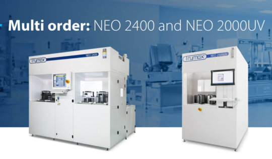
Trymax Receives Multi-System Orders for NEO 2400 Series
NIJMEGEN, THE NETHERLANDS – Trymax Semiconductor Equipment B.V.(Trymax), a global leader in plasma solutions, today announced it has received multi-system...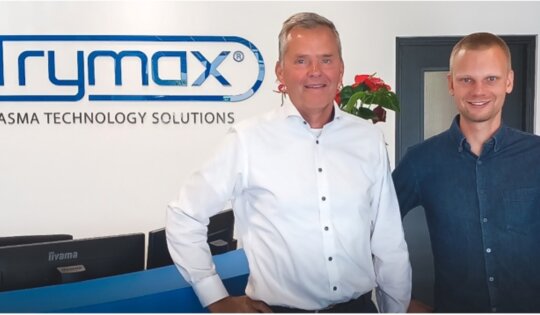
Talking With Trymax About Innovative Plasma-Based Equipment
This interview with Trymax Semiconductor’s Peter Dijkstra, Chief Commercial Officer (CCO), and Karsten Arts, Process Engineer first appeared in Atomic...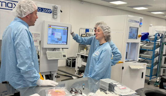
Learning about Plasma Technology Hands-on Through an Internship at Trymax
Hello, I am Mandy Perdok. I am 20 years old and live in Milsbeek in the Netherlands. My hobbies include...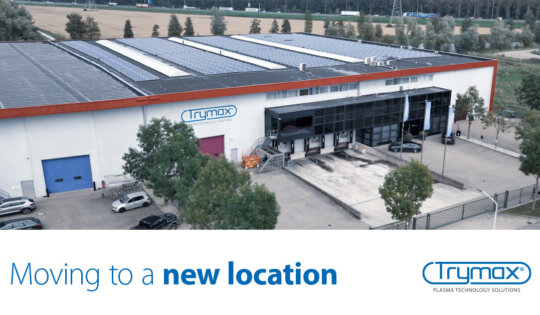
Trymax Moves to a New Green Manufacturing Facility
NIJMEGEN, THE NETHERLANDS – November 8, 2021. Trymax Semiconductor Equipment BV (Trymax), a global leader in plasma solutions for semiconductor...Trymax Wafer Level Packaging DCP™ Plasma Treatment
As semiconductor device manufacturers further shrink the size and increase the reliability of packaging devices, plasma treatment is increasingly used...MEMS Manufacturing: Trymax’ Most Flexible Plasma Ashing Platform
Meet Trymax’ most flexible Plasma Ashing system for running critical low-temperature descum processes and high-temperature bulk photoresist strip processes. These...
Navigating COVID-19 in a Demanding Semiconductor Market
As many of you will agree, 2019 was a very tough year for the semiconductor industry but with a strong...
Scientech Corporation and Trymax Partner to Distribute Resist Ashing and UV Products in Taiwan
NIJMEGEN, The Netherlands and SANTA CLARA, California (Aug. 24, 2020) — Trymax Semiconductor Equipment BV, a global leader in semiconductor...
2020 Outlook: Optimism Ahead! The Opportunities are There
I am writing this viewpoint while 2019 will close in a couple of days. If I try to summarize what...
Trymax Receives Order from a Leading-Edge Photonics Research Organization
NIJMEGEN, THE NETHERLANDS- Trymax Semiconductor Equipment BV (Trymax), a global leader in plasma solutions, today announced it has received an...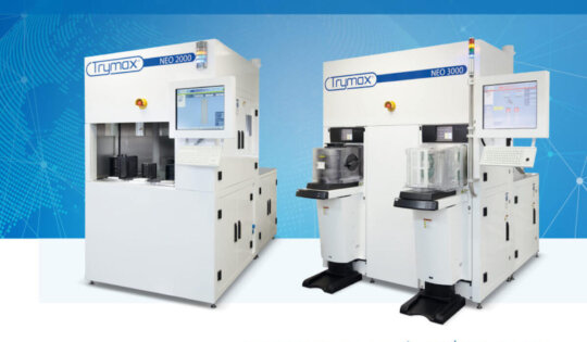
Trymax Receives Multi-System Orders from a Top Ten OSAT
NIJMEGEN, THE NETHERLANDS – May 15, 2019. Trymax Semiconductor Equipment BV (Trymax), a global leader in plasma solutions, today announced...
Trymax Launches New UV Curing and Charge-Erase Product Line
Trymax Semiconductor Equipment BV, a global leader in plasma solutions for semiconductor manufacturers, announces the addition of an ultraviolet (UV)...
Trymax Signs Strategic Financial Partnership with NIBC Bank
Trymax Semiconductor Equipment BV (Trymax), a global leader in plasma-based equipment and solutions for semiconductor manufacturers, is pleased to announce...
Trymax Turns 15 and Celebrates Success at SEMICON Europa 2018
NIJMEGEN, THE NETHERLANDS – November 08, 2018. Trymax Semiconductor Equipment BV (Trymax), a global leader in plasma solutions for semiconductor...
Trymax Receives Multi-System Orders from a Leading Chinese Compound Semiconductor Company
NIJMEGEN, THE NETHERLANDS – October 17, 2018 – Trymax Semiconductor Equipment BV (Trymax), a global leader in plasma solutions, today...
Well-established Advanced Packaging Manufacturer in Taiwan selects Trymax
NIJMEGEN, The Netherlands (March. 02, 2018) – Semiconductor equipment manufacturer Trymax announced today that a Taiwanese establishes advanced packaging manufacturer selects...