Hello, I am Mandy Perdok. I am 20 years old and live in Milsbeek in the Netherlands. My hobbies include playing Netball (Team Sport), training/coaching the Netball youth team, and traveling.
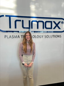
As a third-year student majoring in Chemical Engineering at the Fontys Hogeschool Eindhoven of Applied Science, I am completing my internship at Trymax Semiconductors in Nijmegen.
Trymax was founded by Leo Meijer in 2003. Trymax specializes in designing and building semiconductor equipment for plasma etching. This product line, called NEO, consists of a variety of process chambers and platforms. These range from a semi-automated platform with one process chamber to platforms with multiple process chambers for mass production.
Trymax offers a range of configurable process chambers for plasma technology for all NEO platforms. This allows Trymax to offer a very wide range of processes and options to meet customer requirements.
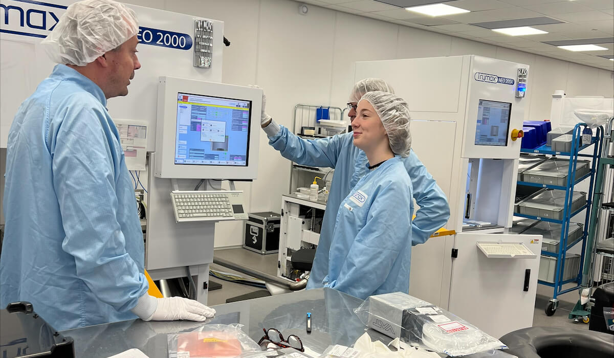
I enjoy working at Trymax with enthusiastic and helpful colleagues. Furthermore, the support from my supervisors at Trymax and at my university is very good. I was well taken care of by my Trymax supervisor, Kyrill Koekenberg, he also introduced me to the world of Plasma etching. He is an excellent tutor and I learned a lot from him.
As part of my internship at Trymax, I studied the impact of plasma damage on the roughness of wafer surfaces subjected to three materials in three different types of process chambers. The characterization of roughness on the wafer surface is carried out on the basis of a Design of Experiments (DoE).

This involves looking at three different plasma reactors and three different wafer layers. The three different plasma reactors include the microwave reactor, the dual source reactor (RF and Microwave), and the CCP reactor. The plasma that is ignited affects the wafer surface. Because three different plasma reactors are used, this means that a different plasma is ignited each time and therefore a different roughness on the wafer surface. The three different wafer layers under investigation are Si, Al, and SiO2. The process parameters that influence the plasma are temperature, power, pressure, and %CF4 in the gas mix. Analysis and measurements are done by using STM, AFM, and SEM.
At SEMICON Europa 2022 in Munich, I got acquainted with other companies in the Semiconductor Industry. It was very educational. As a result, my knowledge of the semiconductor industry has been greatly broadened. Also, I had the chance to mix socially with a lot of people.
The semiconductor industry is an interesting and constantly changing Industry. In the future, I would like to do sales in the Semiconductor industry. Furthermore, I hope there will be more women who choose a profession in technology.