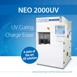
 Trymax Semiconductor Equipment BV (Trymax), a global leader in plasma solutions for semiconductor manufacturers, announces the addition of an ultraviolet (UV) curing and charge-erase product line to its portfolio. The system called NEO 2000UV is a leading-edge dual chamber solution compliant with wafer sizes up to 200mm.
UV curing and charge-erase equipment are used for a wide range of applications that includes photo-stabilization of the resist prior implantation or etch, for small CD, or to erase charge built-up during the IC manufacturing process. This new offer from Trymax will contribute to support the 200mm wafer capacity increase over the period 2019-2022 forecasted by SEMI in its latest report*.
The decision of Trymax to develop such new product was based on the market demand. Several IC fabs were facing difficulties to find UV curing/charge-erase equipment to expand their manufacturing capacity or simply maintain their existing toolset. Customers had to rely mainly on the rarely available refurbished equipment and parts.
“By launching NEO 2000UV, Trymax offers a longer-term perspective to IC manufacturers”, stated Ludo Vandenberk, Executive Vice President of Trymax. “This new product line extends Trymax capabilities to support the semiconductor industry and will generate value for the customer by enabling higher yield in wafer manufacturing.”
NEO 2000UV has been designed taking advantage of the reliable NEO platforms developed by Trymax for plasma ashing, descum, and etching applications. NEO 2000UV is implementing state-of-the-art robotics, components, the latest digital technologies, and software, and is CE compliant. NEO 2000UV can accommodate cassettes or SMIFs. It is manufactured in the Netherlands.
First shipments of pre-ordered systems will start in early Q3 2019. Customers interested to run demonstrations in Trymax application lab are invited to contact Trymax.
Reference
* 200mm Fabs to Add 700,000 Wafers Through 2022, SEMI Reports (Feb 12th, 2019)

About Trymax Semiconductor Equipment BV:
Trymax’s core business is to support semiconductor manufacturers through the world with innovative plasma-based solutions for photoresist removal, surface cleaning, isotropic etch, as well as UV curing/charge-erase, that are used in the fabrication of integrated circuits and other semiconductor devices. Trymax is a privately held company headquartered in Nijmegen, The Netherlands. Trymax operates regional offices in China (Suzhou) and Italy (Milan). Learn more at www.trymax-semiconductor.com.
Company contact:
Yann Guillou
Global Marketing & Sales Director
+31 24 350 08 09
Yann.guillou@trymax-semiconductor.com