
Historically, we all took Moore’s Law for granted. With each new node, we could expect to see faster-performing devices, smaller design footprints and, ultimately, lower design costs. Nowadays these benefits are not clearly achievable for all designers. At the latest advanced technology nodes, we may be able to see faster devices through the miracles of finFET technologies, but do we really get the smaller form-factors? In many cases, the additional rules required for such technologies prevent it. At the same time, the sheer increase in the number of additional masks, coupled with the increased mask costs, makes the cost benefits questionable. For this reason, the industry has begun to explore alternative design practices in an effort to regain some of these benefits. Collectively, these approaches are often referred to as “More than Moore” technologies.
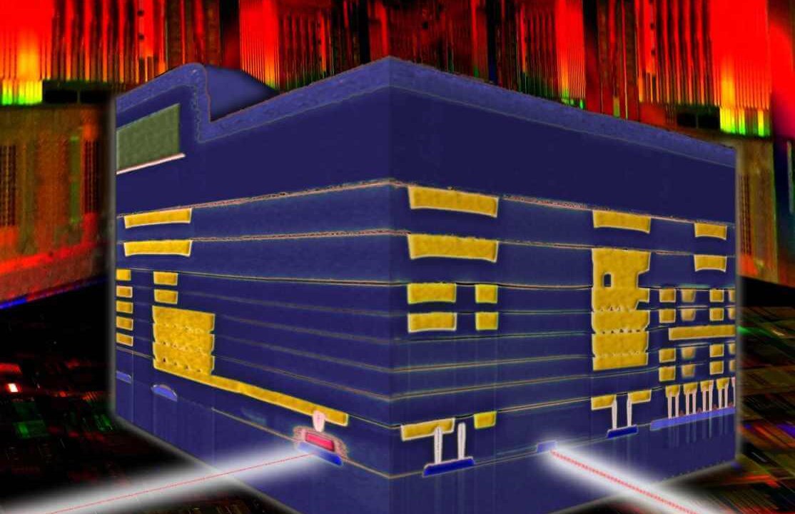
We know that 3D IC design methodologies are one such technology, the goal being to partition what would otherwise be a physically large area into smaller pieces that can be stacked, resulting in smaller form factors, allowing us to pack more functionality into tablets and other hand-held devices. Theoretically, targeting less-expensive process technologies for all but the most critical components can also result in a cost savings, though that is still debatable. But, aside from some novel design concepts (such as the memory cube), typically you will not see a performance advantage. In fact, because stacking requires the introduction of through silicon vias (TSVs) to pass the signal between dies, we may get a performance degradation, along with a power penalty and countless other concerns (compared to a single chip solution).
Another of the More than Moore technologies is silicon photonics. Photonic design is the art of moving and transforming signals in the form of photons, allowing the message to literally travel at the speed of light, and bringing the promise of significant performance gains. Because light signals can pass through each other essentially unimpeded, this also brings the theoretical ability to eliminate the need for vias, dramatically reducing the power required to pass said signal.
As luck would have it, silicon surrounded by silicon-oxide makes an almost ideal waveguide material, meaning the optical signals can traverse with very little degradation. This has raised the possibility that photonics can be designed and manufactured using the same fabs already in place for traditional IC design. But, of course, there is always a catch. The issue for photonics design is that it really is purely passive. If you want to change an optical signal, you must induce that change using either heat or a magnetic field (or both) in the vicinity of the waveguide carrying the signal. Of course, using basic electronics, we already know how to design such controls, so the concept of photonic-electronic co-design sprung up.
So, all we have to do is create a design with some photonics components and some electronics components and we’re done; we simply pass timing-critical data as optical photons and use tried and tested electronics elsewhere, right? Well, maybe not. Depending on the complexity of your electrical configurations, you may need to target those expensive CMOS processes again. Unlike the CMOS transistor, however, there is little benefit in porting a silicon photonic waveguide to an advanced node. That is because the optical behavior for such components is set by the total length and width of the wave guide, along with some other concerns, like bend structures or how close it is to other components. The widths for waveguides in silicon are very large (100-200nm) compared to today’s CMOS devices. So, even if you go to a new process node, the photonics section stays the same size. Sure, you might get a little better lithographic integrity through the printing stages, but is it worth it?
Here is where things may get interesting. If we combine silicon photonic processing with 2.5D processing, then perhaps we can partition the optical components to a less expensive process, such as those typically targeted for interposer use (like, say 90nm), while targeting those more critical electrical components to a die on a more advanced process node, maybe 28nm. Then we may be able to bring together the best of both worlds! This is, in fact, where a lot of photonics research is currently targeted.

Unfortunately, we’re still not there yet. There are lots of questions that still remain to be answered. For example, if we were to create photonics components on a 2.5D interposer, connected electrically to an advanced node die for electric components, then we’re back to relying on TSVs. How much benefit in terms of performance and power will be lost in this trade-off? When we stack the dies, loaded with TSVs, we’ll invariably generate heat and stress. What impact will this have on the photonics components? The photonics will require a laser source, but because we’ve yet to produce a usable silicon laser in standard CMOS process, it will need to sit off-die. What impact will this have on the form-factor? What impact will the heat generated by the laser have on the near-by electronic components?
As you can see, we still have a long way to go. As is usually the case, in uncovering the answers to these questions, we will learn more, allowing us to open up yet further design practices. So while we’re not there yet, there still seems to be a bright future on the horizon. ~ J. Ferguson


