
“How is heterogeneous 3D integration defined?”
There are certainly different understandings in the microelectronics community regarding the definition of heterogenous 3D integration. In a very general definition, it is defined as the 3D integration of different devices such as a CMOS processor and a memory, for example. A more limiting specification would define it as the integration of different substrate materials necessary for the condition (e.g. GaAs / silicon). For the purpose of this article, we will define it as the 3D integration of components with significant different device technologies as e.g. CMOS and MEMS.
Fraunhofer has worked on 3D integration for almost 3 decades. Beginning in the mid 90´s the Munich institute IFT (now EMFT) focused on 3D technologies for the use of known good dies by chip-to-wafer stacking (and was, at the time, competing with wafer-to-wafer-stacking). Understanding the necessity for combining research on both 3D technology and design at an early stage, we established a fruitful cooperation between the two Fraunhofer institutes in Munich and IIS-EAS Dresden.
3D integration is now considered to be a new paradigm for the semiconductor industry. There are various ways to vertically interconnect devices, with most advanced technology based on through-silicon vias (TSV).¹ Within wafer level packaging (WLP), the platforms using TSVs are 3D IC integration and interposers (“2.5 D”). Silicon interposer technologies are already mature and used in several production lines. The situation is different when it comes to “true” 3D ICs. The first companies are just beginning to take the step to production of 3D integrated products. This also provides a motivation to investigate the 3D IC patent situation.
As expected, IBM, Samsung, Micron, TSMC, Hynix and STATS ChipPAC are the leading players concerning the number of patents held. On the other hand, relevant patents on 3D integration are also found among different academic institutions with ITRI being the top institute, followed by CEA (France) and Fraunhofer-Gesellschaft München (Germany). Apparently Europe is strong in intellectual properties for 3D ICs. World-wide, memory-enhanced applications are seen as the main driver for 3D Integration.
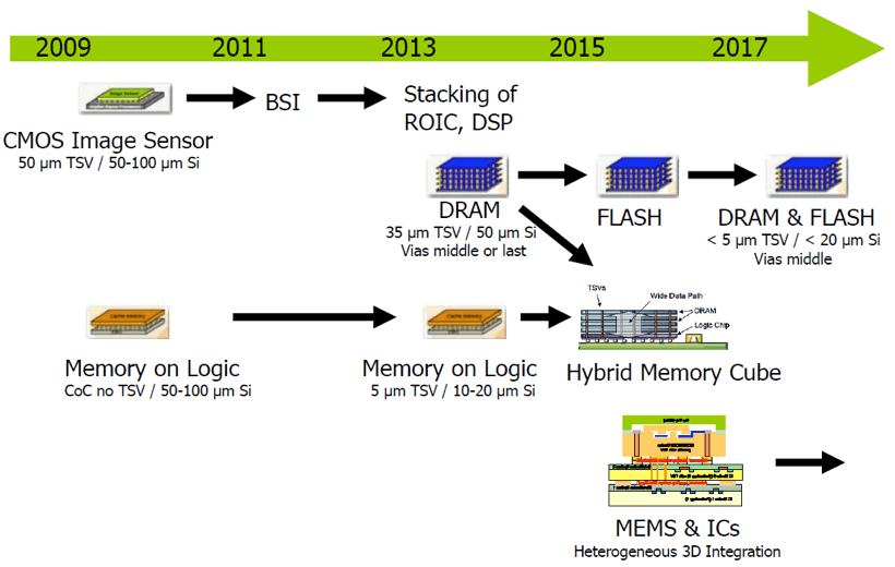
According to revenue forecast surveys by Yole Développement, heterogeneous MEMS/IC systems could become the driving markets for 3D-TSV integration with a predicted demand for MEMS with 3D TSV of several hundred thousand wafers a year by 2015.² With the maturity of heterogeneous 3D integration technologies and corresponding low-cost fabrication, a diversity of 3D integrated CMOS-MEMS products will be developed, leading to a further key application track (Figure 1).
“What is needed for Heterogeneous 3D Integration Technology?”
3D ICs are certainly the key enabler for 3D heterogeneous systems. Moreover, specific requirements include highly-reliable and robust processes for stacking, vertical interconnections for fully processed devices by wafer-level 3D integration of known good die (KGD), and provision of very small form factor and fine-pitch vertical interconnects. In particular, 3D TSV technologies with freely selectable TSV positions have a strong demand for 3D system design methods to enable high-performance of extremely miniaturized heterogeneous systems. The technology developments will have to deal with the following three basic conditions for heterogeneous integration. The components to be integrated will in general:
- Be fully-processed devices (e.g. ICs with different complex backend-of-line layers, sophisticated MEMS/NEMS or antennae devices)
- Exhibit different chip areas
- Not necessarily be fabricated with very high wafer yield
As a consequence, robust and reliable 3D technologies based on chip-to-wafer stacking of KGD are needed. To supply solutions for these requirements the European e-BRAINS consortium established the 3D Heterogeneous Integration Platform where technologies of the following relevant main categories* of 3D Integration are provided to enable future applications of smart sensor systems.³
- 3D System-on-Chip Integration – 3D-SOC: TSV technology for stacking of thinned devices or large IC blocks (global level)
- 3D Wafer-Level-Packaging – 3D-WLP: embedding technology with through-polymer vias (TPV) for stacking of thinned ICs on wafer-level (no TSV)
- 3D System-in-Package – 3D-SIP: 3D stacking of packaged devices or substrates
Regarding TSV performance, the applications do not need ultra-high vertical interconnect densities as for 3D stacked Integrated Circuits – 3D-SIC*. Nevertheless, the lateral sizes of the TSVs are preferably minimized to allow for place and route for small “open” IC areas. Smaller TSVs are also preferred to reduce thermo-mechanical stress.
e-BRAINS’ focus is on how heterogeneous integration and sensor device technologies can be combined to bring new performance levels to targeted applications with high market potentials. The consortium, under coordination of Infineon and technical management by Fraunhofer EMFT, comprises major European system manufacturers (Infineon, Siemens, SensoNor, 3D Plus, Vermon and IQE), SMEs (DMCE, Magna Diagnostics, SORIN and eesy-ID), the large research institutions CEA Grenoble, Fraunhofer (EMFT Munich & IIS-EAS Dresden), IMEC, SINTEF, Tyndall and ITE Warsaw, and universities (EPFL Lausanne, TU Chemnitz and TU Graz). Target applications include automotive, ambient living and medical devices, with a specific focus on wireless sensor systems.
The e-BRAINS partners are working close together to enable the 3D Heterogeneous Integration Platform. Infineon, Fraunhofer EMFT, IMEC and SINTEF are focusing mainly on 3D-SOC and 3D-WLP, while the French system manufacturer, 3D Plus, and Tyndall are focused on 3D-WLP and 3D-SIP technologies.
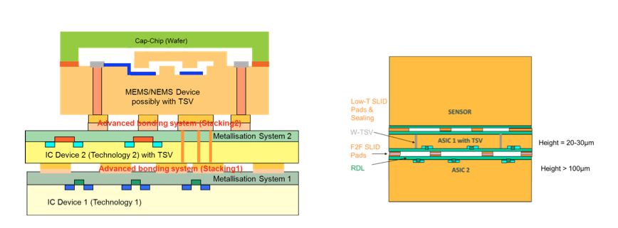
In future sensor systems components, such as for the Internet-of-Things (IoT), application-specific ICs and sensors will be integrated using dedicated 3D heterogeneous integration schemes. A 3D architecture of a wireless sensor system, for example, contains typically at least two IC devices: a sensor read-out and a communication ASIC (FIgure 2a). Figure 2B, shows an IoT-relevant application example that implements additional security features to hinder essentially manipulation and misuse of secret/private data and counterfeiting of components (Fraunhofer EMFT patent pending): the robust face-to-face metallization is realized by intermetallic compound (IMC) bonding of the two ASICs. The sensor is connected by tungsten-filled TSV through the ASIC 1. IMC bonding by Solid-liquid-interdiffusion (SLID)⁴ is used to mechanically and electrically interconnect the MEMS and IC devices in a robust and reliable way, as well as ensure sealing of the complete MEMS/IC stack.

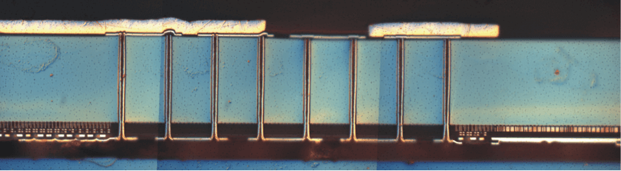
Fraunhofer EMFT´s 3D-SOC technology “TSV-SLID” can be applied to completely fabricated devices and fulfills the requirements for heterogeneous products described above. In this technology TSVs are processed through all exposed layers of the IC (Si and dielectrics). The complexity of corresponding processing for vertical interconnects can be seen in a cross section of an ASIC with 7-level metallization and tungsten-filled TSV prepared for device stacking (FIgure 3). Ultra-fine pitch W-TSVs (lateral dimension 1-2µm) are used for the 3D-SOC process, because of reduced built-in stress, full CMOS compatibility and particularly the established production capability – obviously until today only 3D IC integration based on W-TSV has been used for production (e.g. at Tezzaron and IBM).
(Source: Fraunhofer EMFT)
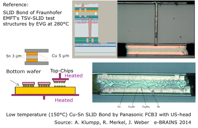
Substantial progress beyond the state-of-the-art in 3D integration is needed especially for sensor applications and has been achieved within the e-BRAINS project. One of the key issues for heterogeneous systems´ production is the impact of 3D processes on the reliability of the product, i.e. the high built-in stresses caused by e.g. the CTE mismatch of complex layer structures (thin Si, inter-metal dielectrics, metals etc.) in combination with elevated bonding temperatures. In simplified terms: the lower the process temperatures, the lower the stress issues. As a consequence, Fraunhofer EMFT focusses on the development of highly reliable low-temperature bonding for 3D heterogeneous integration.
A new IMC bonding technology was developed using ultrasonic agitation in a Panasonic FCB3 Bonder to reduce the assembly temperature below the melting point of tin (Figure 4). Robust die-to-wafer bonding at 150°C has been demonstrated based on Cu/Sn metal system, with shear forces of 17 MPa and alignment accuracy of 3µm.⁵
“What is the range of applications?”
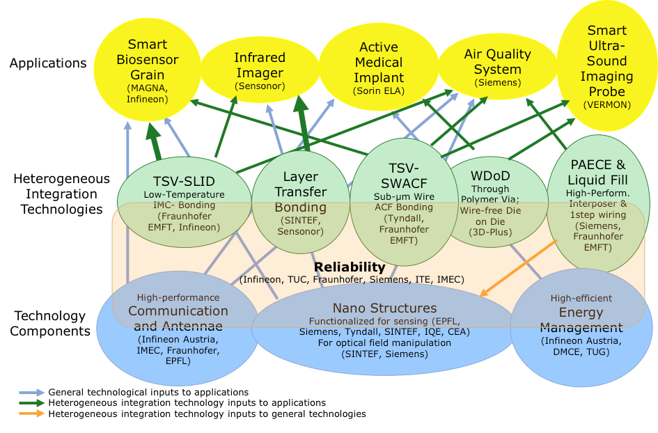
In general, all fields of ambient assisted living, smart buildings (e.g. wireless gas sensors for air quality systems), safety and security (e.g. IR imagers), biosensors and smart medical systems as e.g. active medical implants are all foreseen applications. Figure 5 shows the key applications targeted in the e-BRAINS consortium and their enabling heterogeneous 3D technologies.
The main driver of 3D heterogeneous integration is certainly sensor integration. The system integration of sensors with ICs and passive components, as energy harvesters, actuators and batteries, is becoming more and more important especially for the high growth market area of distributed wireless sensor systems, which will constitute the key connected hardware infrastructure of the IoT.
*definitions according to Ref. 1
References:
- P. Garrou, M. Koyanagi and P. Ramm: “3D IC Integration”, Handbook of 3D Integration, Vol. 3, Wiley-VCH, 2014 (ISBN: 978-3-527-33466-7).
- 2 R. Beica, J.-C. Eloy and P. Ramm: “Key Applications and Market Trends for 3D Integration and Interposer Technologies”, Handbook of 3D Integration, Vol. 3, Wiley-VCH, 2014 (ISBN: 978-3-527-33466-7).
- “Best-reliable ambient intelligent nanosensor systems by heterogeneous integration – e-BRAINS”, granted by the European Commission under grant agreement no. ICT-257488; project coordinator: Infineon Technologies; www.e-brains.org
- P. Ramm, J.-Q. Lu and M.M.V. Taklo: “Introduction to Wafer Bonding”, Handbook of Wafer Bonding, Wiley-VCH, 2012 (ISBN: 978-3-527-32646-4).
- Taklo, M.M.V.; Schjolberg-Henriksen, K.; Malik, N.; Tofteberg, H.R.; Poppe, E.; Vella, D.O.; Borg, J.; Attard, A.; Hajdarevic, Z.; Klumpp, A.; Ramm, P.: “Low-temperature bonding technologies for MEMS and 3D-IC,” 4th IEEE International Workshop on Low Temperature Bonding for 3D Integration (LTB-3D), 2014, p.34