


SUSS, being an equipment maker addressing various manufacturing challenges faced by 3D IC enablement, definitely has a lot riding on ensuring that all pieces of the 3D IC puzzle are in place. This was evident from the range of presenters they had lined up during this year’s Technology Forum, held at the The St. Regis San Francisco, 125 3rd St, San Francisco, as part of the company’s SEMICON West program. As far as I was concerned, what would have normally been a relaxed attendance of technical presentations aided by coffee and scrumptious cookies turned out to be quite a feverish session of notes taking due to Françoise’s request to summarize the event.
Fast forward 24 hours, I sat down to finish up a nice little summary of the event. The moment I looked into the technological details in my notes, all hopes of ‘littleness’ vanished from the summarization task. Then I remembered someone once telling me that a picture was worth a thousand words. What you see in Figure 1 is the 3D IC packaging process flows along with a few of the major forks one could take along the way. While this picture itself is not from the speakers, I have captured the maturity status conveyed by them for many of the process steps in the color coded boxes (Green for mature to dark red for evolving areas and other colors in the spectrum falling in between). The speaker who covered the topic is also annotated in the image. Eric Beyne (IMEC), Ron Huemoeller (Amkor) and Jon Greenwood (GLOBALFOUNDRIES) covered most of the high level flow enablement topics.
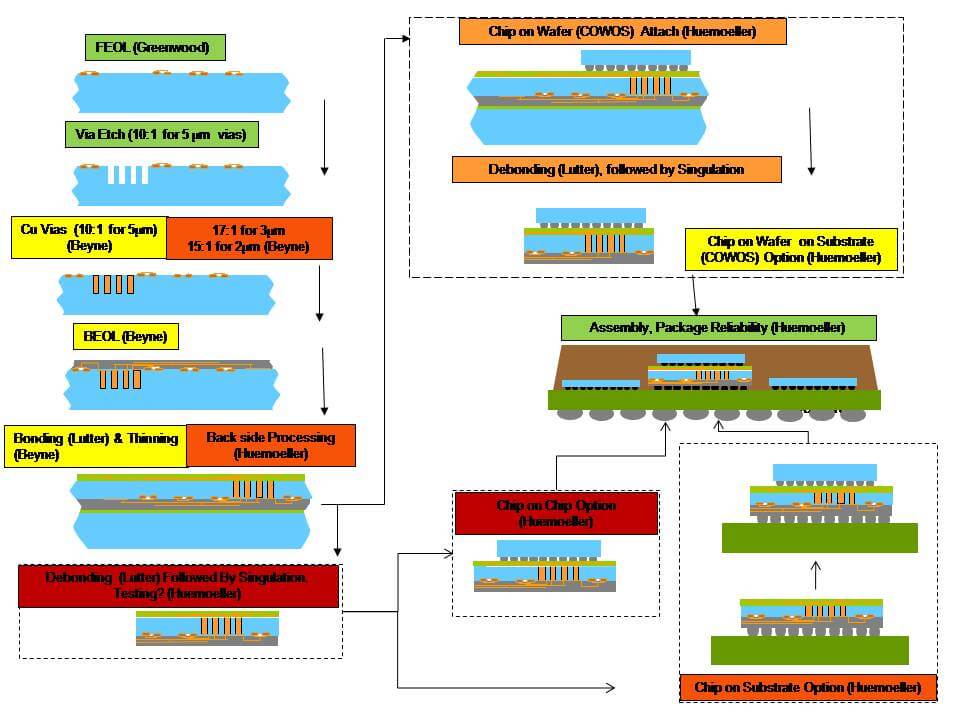
Figure 1: 3d IC Packaging Flows and Process Challenges Presented by Speakers at the SUSS Technology Forum (Click on image for enlarged View)
The afternoon session kicked off with an excellent overview of the roadmap and challenges at all levels of the 3D and 2.5D enablement from none other than Eric Beyne. In today’s climate of super-secrecy and tight lipped public statements ruling the microelectronics landscape, Eric’s presentation was a surprisingly detailed spelling out of many of the hurdles in the 3D IC roadmap. In his presentation, Eric identified copper stabilization as an important issue to be understood in ensuring BEOL, as well as new technology node reliability. Eric’s presentation went beyond immediate challenges and into future challenges in the roadmap. In this context he also talked about thinner dies with smaller TSV diameters (2µm and 3µm). Shrinking of TSV diameters driven by technology node shrinking, also leads to the need for chip-to-chip interconnect shrinking. This context naturally lead his presentation to micro bumps, pillars and copper nails as the next progressive steps as the interconnect pitch shrinks.
When the next speaker Ron Humoeller of Amkor started off by saying that this is not business as usual, he set a tone of practicalities, and dollars/cents associated with making 3D IC a viable technology. Between that start, and a conclusion which identified FPGA, ASIC, graphics as the immediate target areas for 3D/2.5D technologies, followed by mobile adoption only after significant cost reduction, Ron identified a number of technical challenges and how they have been overcome. The speech projected a technologically encouraging picture with interim testing, thin wafer handling, and backside processing as some of the challenges. In this context, Ron’s speech lingered shortly on the topic of Chip on Substrate (COS), Chip on Wafer on Substrate (COWOS) and Chip on Chip approaches. Ron identified Chip on Substrate as an interim test-friendly flow, since existing BGA-array-level probing can be utilized for interim test.
Jon Greenwood also stressed GLOBALFOUDRIES’ mantra of collaborative development. In addition to offering insights into the Globalfoundries Technology Development Center, and GF’s commitment to doing it together with supply chain partners, Jon projected that foundries as well as the OSATs are ready to serve the industries 3D IC needs by 2015.

Stefan Lutter (SUSS Microtech), Michael Gallagher (Dow Chemical) and Alexander Smith (Brewer Sciences) talked about temporary bonding and debonding technology and equipment. Stefan’s presentation addressed high level classification and viability of the different debonding processes, namely solvent release, thermal sliding, laser release and mechanical debonding. After a methodical evaluation of process throughput and bump-damage-related yield concerns, Stefan cast his doubts about the suitability of the first two for 2.5D and 3D. In his opinion laser, and mechanical debond processes were viable. He went on to talk in more detail about the mechanical release and SUSS equipment platform. Michaell Gallagher talked about thermal stability of bonding materials and Alexander Smith from Brewer Sciences discussed temporary bonding material requirements using a case study of three unnamed customer situations.
Interesting, even though featuring outside of the above connected process flow is the topic of Glass interposers for 2.5 D integration. Vern Styger of Asahi glass did a good job of positioning glass based technology roadmap. Simplistic metrics such as TGV diameters, and interposer thicknesses achievable from the technology seemed higher than what is achievable with silicon. Vern positioned glass as a long-term solution for very high frequency applications due to its low insertion losses, and for optical electronics. He projected 2015 to 2017 as the time frame by which industry will be ready for glass sheet based processes. Vern believes that by then glass will be the low enough in cost to meet the industry’s cost targets. ~ KK


