
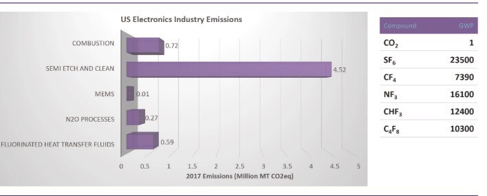
A significant amount of the focus on sustainability in the semiconductor space is on Scope 2 and Scope 3 emission. We’re either working to reduce the energy required to run the factories that produce semiconductors and semiconductor manufacturing equipment, or the greenhouse gases (GHG) produced once the semiconductors or equipment have been shipped to an end user. While, a significant amount of semiconductor greenhouse gas emissions is the result of the energy required to heat, cool, and process wafers, there are also chemicals used in the process that have a considerable GHG impact that typically fall in the scope 1 category. Figure 1 shows the impact of the major GHG chemical bad actors used in the semiconductor manufacturing industry, particularly in etch and clean.
The chemistries used to produce semiconductor chips fall into Scope 1 or Scope 3 emissions. While these chemicals have a very significant GHG footprint, fortunately, most of the exhaust from an etch system runs through an abatement system, and then subsequent scrubber. This minimizes the impact; however, abatement systems are not 100% effective and some gas makes it through the system. Abatement is also energy intensive, which adds to the greenhouse gas emissions problem. GHG gases can also be leaked when manufacturing, installing, and transporting.
Another concern that has emerged is with Perfluorinated Alkyls or PFAS chemicals. Resolving it will be a major challenge for the semiconductor industry. In etch processes with high-aspect-ratio etches or where high selectivity is needed, polymers are formed, that when removed during the cleaning process, likely have some PFAS as a by-product. Health and environmental organizations are working to limit and reduce the use of PFAS worldwide. This will have a significant impact on the semiconductor industry as the chemistries used for etching and other processes will be significantly transformed.
Changing chemicals in the semiconductor process is no easy task. For many years, the processes using high greenhouse-warming-potential (GWP) chemistries have been fine-tuned, and are well understood. Introducing new chemistries requires years of development to first create or identify in the lab, and then to test and evaluate to ensure there will be no damage to the final semiconductor product. Removal of chemicals such as PFAS from the waste stream is extremely challenging. Fortunately, the industry is acknowledging the GHG and chemistry problems and is stepping up to the challenge.
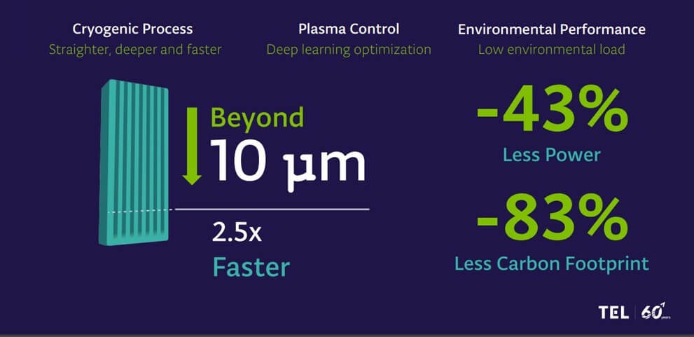
At Semicon West 2023, sustainability was a major focus of the show. During the CEO keynote session, TEL’s Tony Kawai laid out a significant part of the company’s sustainability focus, but more importantly, Kawai announced a new high aspect ratio etch process that significantly reduces both energy and the CO2 footprint of the etch (Figure 2). The etch is performed at cryogenic temperatures, and uses an alternative chemistry to the current process. Kawai claimed that the etch is 2.5x faster, uses 43% less power and reduces GHG by 83%. This is a significant breakthrough. It will be interesting to see the adoption rate of this new etch process, and even more interesting to see if the new etch chemistry is shared with other etch companies.
Prior to SEMICON West, EMD Electronics posted a blog titled Investing in a Sustainable Semiconductor Future: Materials Matter. It discussed GHG emissions and some of the challenges they are addressing in looking at how to reduce GWP by changing chemistries.
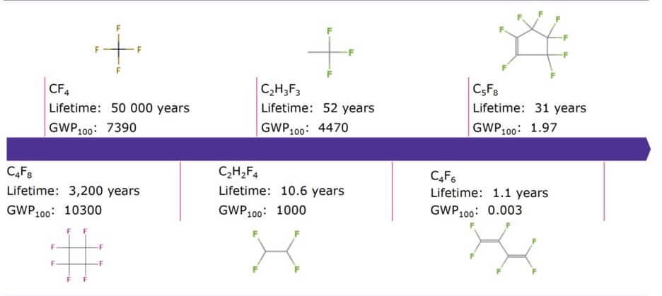
The fluorocarbon you choose to etch your material can have a significant impact on your company’s GHG emissions. Figure 3 shows the lifetime of some typical etch fluorocarbons and the GWP of the molecules. So, if you could replace CF4 with C4F6, it would make a huge impact on the GHG emissions of the semiconductor industry. The EMD electronics blog points out that changing chemistries is not trivial, but you have to start somewhere, and to meet carbon-neutral goals by 2030, a change in chemistries would go a long way to help.

Both semiconductor equipment and chip manufacturers rarely tip their hands when it comes to process changes or process improvements. However, if they are serious about collaboration to reduce the industry’s carbon footprint, we should start to see more cross-industry dialogue regarding the removal of GHG from the manufacturing lines, and the potential for cross-licensing of technology to help reduce the GHG footprint.
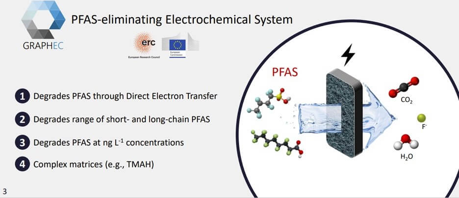
On the PFAS front, how to replace these chemicals is causing a bit of a scramble. PFAS are crucial to the semiconductor process, and unfortunately, they make their way into the environment. At the SEMICON West S3 Summit, Graphec, an S3 startup, is looking at methods for removing PFAS from the waste stream. Graphec passes the waste stream through an electrochemical system that its lab scale studies eliminate about 77% of the PFAS materials. I hope the S3 venture groups can scale this technology successfully and quickly, not only for the semiconductor industry but also for the removal of PFAS from the environment.
The semiconductor industry has always been a source of innovation for creating new processes, and technologies. It’s good to see that the industry is applying its innovative resources to solving not only the semiconductor industries’ GHG and waste stream issues, but also looking at the broader GHG and materials issues facing us all.


