
IMAPS‘ inaugural CHIPCon 2023 – the reinvention of its Advanced SiP Conference – took place July 24-27 in San Jose. Right out of the gate, it reminded me of the early days of RTI’s 3D ASIP Conference that I attended for nine straight Decembers in Burlingame, CA. The single-track format was similar. The same advanced packaging technology pioneers showed up to present and network. We asked the same questions about die-to-wafer hybrid bonding that we asked about through silicon vias (TSVs). We talked about the importance of chip-package co-design. And we argued about what differentiates chiplets from multi-chip modules.
But there was one significant difference. Rather than focusing only on applications, process technology development, and supplier solutions, CHIPCon brought together the entire chiplet ecosystem, from design all the way through to test and standard protocols. It’s almost like we learned something from our past: that bringing new technologies to the market requires collaboration. And it was great.
Chiplets and the CHIPS and Science Act
One thing is for sure; we’ve definitely got the attention of the U.S. government. In his keynote, IBM’s Scott Sikorski set out to unravel, once and for all, the mysteries of the key players and programs through which U.S. companies can tap into government funding. These include the National Advanced Packaging Manufacturing Program (NAPMP), the Electronics Resurgence Initiative (ERI 2.0), the Next Generation Microelectronics Manufacturing Program (NGMM) the Defense Procurement Act (DPA) The Strategic Transition of Microelectronics to Accelerate Modernization by Prototyping and Innovate in the Packaging Ecosystem (STEAMPIPE), and Microelectronics Commons.
In addition to his day job at IBM Research, Sikorski is part of the American Semiconductor Innovation Coalition (ASIC – catchy, right?) comprising 200 entities that are interested in participating in the research arm of the CHIPS Act, Section 9906. Along with SEMI’s Melissa Shemansky, he led the advanced packaging workstream.
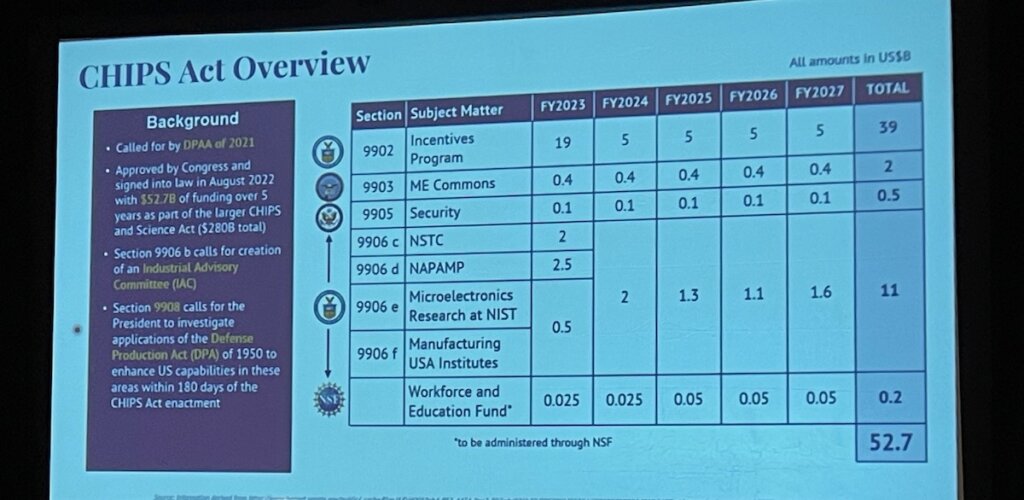
There was a lot to unpack, and Sikorski clearly did his research. He explained that out of the $52B earmarked for the CHIPS Act portion of the CHIPS and Science Act, $11B goes to fund 9906, and out of that bucket, $2.5B goes to fund the NAPMP. It’s a substantial sum, and all of it is available in year one (Figure 1).
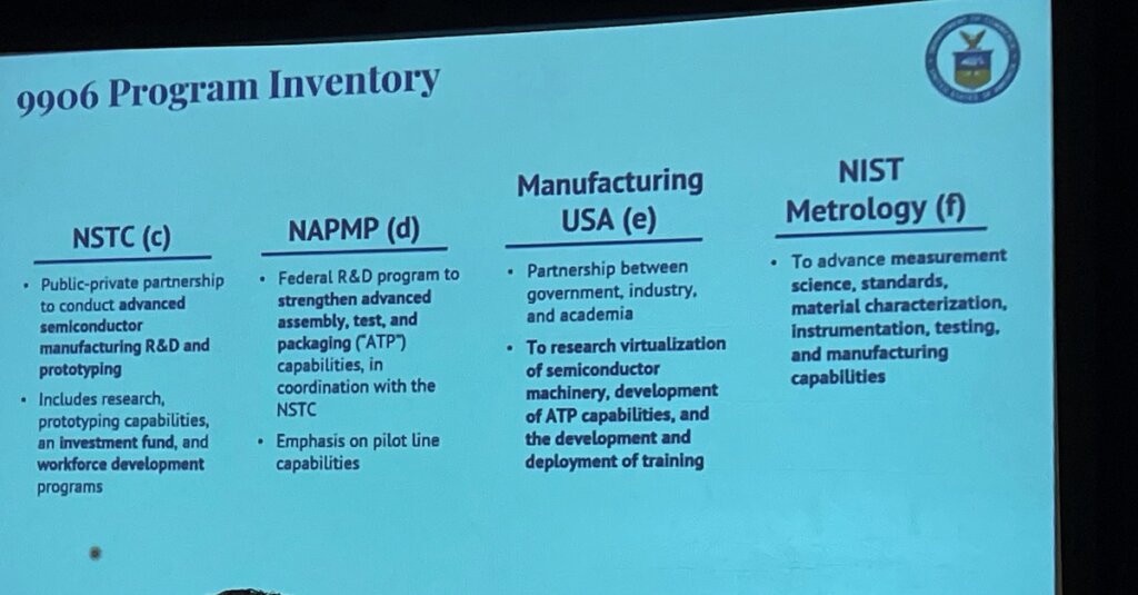
Sikorski’s detailed presentation outlined the different organizations and programs; and the opportunities each of them offer. (Figure 2). He explained that not all of them are tied to the $52B CHIPS Act funds. Some are already funded by initiatives like the DoD’s Rapid Assured Microelectronics Prototypes (RAMP) and State-of-the-art Heterogeneous Integration and Packaging (SHIP) initiatives.
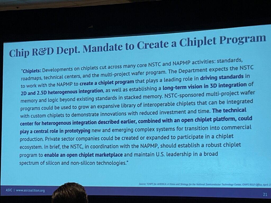
Most important for this audience was the CHIP R&D Department’s mandate to create a chiplet program. (Figure 3)
In a 3D InCites podcast interview that will drop on Thursday, August 10, Sikorski explained to me that this $2.5B is an R&D funding stream. There is also the $39B CHIPS Act section 9902 monies earmarked for incentive programs, such as building greenfield or brownfield retrofits of commercial advanced packaging facilities onshore.
However, the money is for investment in the facility only, not for ongoing expenses. Sikorski explained that this is the main challenge for reshoring advanced packaging because these facilities would be operating at a 20-30% penalty doing production in America compared with Asia.
Another important takeaway from Sikorski’s talk was some basic ground rules for accessing the funds. We can’t spend the money on “countries of concern” – it needs to stay in country and/or friendly countries. It also can’t be used for “financial engineering and gimmickry” such as stock buybacks. The third significant restriction – the prohibition on doing business in China for 10 years.
The bottom line is anyone in the packaging space should take the time to educate themselves about these programs because it’s a once-in-a-generation opportunity. If you have access to the deck Sikorski shared, it’s a comprehensive resource. Check with IMAPS to see if it’s available.
And while we still don’t have a solution for onshore packaging at scale, Sikorski does see a path forward for DoD needs. But the DOC is trying to solve a bigger problem, which is, “how do we go from 3% of packaging to something somewhere in the teens. And how do we make it economically sustainable – that hasn’t been addressed yet.” he said.
Technology Takeaways from CHIPCon 2023
The keynotes and panel discussions shifted to technology topics, beginning with Vincent Kim, of Samsung. He announced that Samsung believes that the solution to the cost, performance, and memory bandwidth challenges we face can be solved with advanced packaging.
With all the functionality packed into them to support advanced needs of not only high-performance computing (HPC) and networking but also artificial intelligence (AI) and machine learning (ML), today’s system-on-chip (SoC) architectures are reaching reticle limits. Chiplets are the solution. But there’s a need for high performance, low-power interconnect between chiplets, explained Kim.
He described different solutions for 3D stacking, from lower-price microbumping using thermocompression bonding, to bumpless interconnect made possible by hybrid bonding. He also talked about putting HBM on top of the logic die and replacing SRAM with LLC DRAM on top of the logic.
“We are clearly now in the 3D IC era,” said Kim. “All this work of the past 20 years is finally coming to fruition and Samsung is rolling out an end-to-end ecosystem we call Samsung AVP.”
It includes investment in heterogeneous integration, chiplets, and even test. Kim invited attendees to “Bring your own architecture and focus on core ideas.”
From Youngsu Kwon’s (ETRI) presentation, Petaflops AI Neural Processor on Chiplet Heterogeneous Integration Package, it was fascinating to see how many mathematical calculations go into developing an AI chip.
From Kevin Rinebold, Siemens, we learned that disaggregation has disrupted traditional EDA tools and methods, as well as caused changes to the supply chain. We now need to transition to system-based design from design-based optimization. He talked about the importance of balancing design resources across competing multi-domain requirements.
Zain Ali, Intel, explained how EMIB allowed for disaggregation of an SoC into chiplets to heterogeneously achieve the performance of a monolithic SOC. He said it is the optimal solution for integrating high bandwidth memory (HBM) with chiplets. Here would be a good place to point out that HBM itself is NOT a chiplet scheme. It is 3D stacked memory die using TSVs.
Cadence’s John Park noted that the needs of IC and system designers are converging to force engineers to develop co-design methodologies. “Co-design breaks down the walls of over-the-wall design methodologies,” he said. We’ve been talking about it for decades. In my opinion, this is a long time coming.

From Jeff Cain we got a tiny peek at Chipletz – an early-stage startup that spun out of AMD. It’s headed up by Bryan Black and Michael Su, known for being instrumental in HBM, and for their work on AMD’s Fiji processor and EPYC. Because the company is still in stealth mode, Cain’s presentation focused on the toolset flow that the worked with Siemens on to get the unique package design that Chipletz is.
Besi’s Tom Strothman presented the afternoon keynote on hybrid bonding. We’ve covered this topic exhaustively over the past few months, so I won’t go into detail here. But he set the stage for some presentations on new developments.
As an alternative to die-to-wafer hybrid bonding, Peter Van Emmerick, of Kulicke & Soffa presented a fluxless approach to thermocompression bonding (TCB) using formic acid oxide reduction in situ pre-cleaning as well as during the TCB process. He presented a yield and package cost comparison of TCB versus hybrid bonding, noting that TCB is much less sensitive to particles, making it more OSAT-friendly than hybrid bonding, which requires front-end cleanliness. The company is working with the UCLA CHIPS program to develop this approach. Subu Iyer talked about it in a recent podcast episode.
Ryohei Ooishi, of Ajinomoto Fine-Tech, discussed the next generation of ABF, a standard dielectric material used as an insulating film for build-up substrates. Nanofiller delivers finer lines and spaces and is ideal for high-density panel-level packaging. It provides a smoother surface and smoother via walls. The company is also developing a sheet molding compound for molding applications that eliminates warpage. Target uses include fanout wafer level and panel level packaging.
Discussing whether Qualcomm would be extending Moore’s Law with chiplet innovation, Jihong Choi, Qualcomm was right on brand with Qualcomm’s message. When it comes to chiplets for the mobile and edge device industry, it’s all about a “cost-effective solution.” While touting the performance benefits of chiplets, Choi pointed out that mobile devices are more price sensitive in the market. The status for 3D chiplets at Qualcomm is pathfinding to define the processes of record. The call to action? It’s important to develop a cost-effective solution for integrated chiplets.
Are Chiplets the Answer for AI?
The panel discussion led by Jan Vardaman addressed the question, “Are chiplets the answer for AI, ML, and Photonics/co-packaged optics? Panelists included Amkor’s Mike Kelly, ASE’s Ou Li, AMD’s Ivor Barber, Intel’s Swadesh Chaudrey, and Chong Zhang of photonics start-up, Ayar Labs.
All panelists agreed that the main motivation to move to chiplets was cost – and we’re not talking about advanced packaging cost here, we’re talking about comparison with the cost of SOCs.
Barber explained that AMD uses a power-performance area and cost matrix to balance whether to go to chiplets for a certain application or stick with a monolithic SoC.
Kelly noted that time-to-market is another key driver and that while applications are starting out in high-end areas like HPC and data centers, they are expected to trickle down to every compute class, including automotive. Li cited network switching and edge computing as other viable markets.
When asked about the challenges with chiplets, Chaudrey said that in terms of packaging different chiplets from different technology nodes, there are no show-stoppers that can’t be overcome. Barber cited thermal management as the biggest concern. Kelly said power density is trending upward as more functionality and transistors are put in a single package. Li pointed to warpage and test as concerns. “We need to have enough known-good-die and known-good-modules to make good yield,” she said. “We are adopting and implementing system-level test to address that.
Since photonics is a different animal, the challenges are different for Ayar Labs, which manufactures photonics-based optical chiplets. Chong noted that photonics IO is more efficient. For them, the major challenge is a mature ecosystem.
Other than this optical chiplet, nobody could name another third-party off-the-shelf chiplet. That’s because there isn’t an open interface yet to make them interoperable.
There was lots of discussion on standards, and different interfaces. We hear a lot about the Universal Chiplet Interconnect Express (UCIe). Still, other interfaces exist as well, such as Intel’s Advanced Interface Bus (AIB), Bunch of Wires (BoW), and AMD’s Infinity Fabric, to name a few.
Jan summed it up nicely in her closing comments:
“We can say we’re at the beginning of our journey with chiplets. We’ve got more to do on standards. We need to include every sector and the defense people and address lots of challenges in design. Test solutions need work. It doesn’t look like assembly is a big issue – unless you want to do hybrid bonding. We’re getting close to seeing some third-party chiplets. It will take more meetings and discussions like this. When it comes to thermal and KGD – we’re going to talk about this until the end of time.”
Now if everyone could just agree on what chiplets are, we’d be all set. Peace out, everybody! ~FvT


