

 Once a month, MEPTEC, now managed by Ira Feldman, organizes a very informative luncheon at SEMI in Milpitas. On November 13, 2019, two well-known industry experts, Anand Joshi and Tom Dillinger, addressed today’s hot topics —neural networks and System-on-Chip (SoC) design challenges — with short, but very informative presentations.
Can We Build Neural Networks That Solve AI Chipset Power Issues?
Anand Joshi, an independent consultant and industry executive, has been working on artificial intelligence (AI) topics since 2014. His presentation’s title was: “Semiconductor Processing Challenges Posed by Burgeoning AI Chipset Markets.” First, Joshi outlined the limitations of Moore’s Law and current computer architectures, then explained why the performance per Watt of our traditional computing solutions are insufficient. Then he gave an example and showed what Nvidia, a dominant leader in power-efficient computing solutions, can achieve today: A 16 GPU computer that consumes 10 kW of power. That’s equivalent to the power consumed by five single-family homes. A data center with only 1000 of these computers requires 10 MW just to power these advanced computers. Cooling requirements and other overhead increases this number even further and clearly encourages us to look for a new paradigm.
The neural networks in human brains consume only about 20 Watts of power. This excellent performance per Watt has encouraged scientists to deploy neural networks in computers – with remarkable success. However, their multi-stage and highly parallel architecture require many cores to be tied together closely, to significantly improve performance per watt. To give an example of implementing neural networks power-efficiently, Joshi showed how Cerebras’ wafer-scale integration approaches this challenge today. (FYI: Cerebrum is the Latin name for the human brain) (Figure 1).
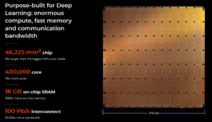
This wafer-scale integration “die” for neural networks is 57 times larger than today’s largest GPU die and is built using TSMC’s 16 nm process. Power is supplied to these many cores from the back. A water-cooled heat-plate cools this large piece of silicon from the top. To improve yields, Cerebras enabled redundancy, using a smart interconnect network. How to develop software for running this chunk of silicon, how to test it and what kind of package it needs were not discussed during the November 13 luncheon.
If you want to listen to Joshi’s entire presentation and see his slides, go to the MEPTEC Presentation Archive.
Dillinger’s Top 10 SoC Design Methodology Challenges
The second speaker was Thomas Dillinger, an experienced designer of high-end SoC and an expert in developing EDA tools and flows. Dillinger worked for 30+ years at AMD, IBM, and Oracle, writes for Semiwiki and recently published VLSI Design Methodology Development, a very comprehensive and up-to-date eBook for System-on-Chip (SoC) and System-in-Package (SiP) designers (Figure 2).
His presentation, titled “SoC Design Methodology Challenges for Advanced Process Nodes” focused on very important topics that our industry needs to address, to meet new and increasingly diverse market requirements. Dillinger must have also enjoyed David Letterman’s late-night television talk shows because he also arranged his message into “Top 10” and counted down to the most important topic.
Unfortunately, none of these “Top 10” were funny! They made me increasingly more worried! I hope that EDA and design experts will take Dillinger’s visionary message to heart and remove or at least lower these barriers over time to increase their own and their customer’s opportunities for profits.
Every one of Dillinger’s top ten future challenges deserves in-depth coverage – beyond the scope of this blog. If you find the topics I briefly summarize below important for your and your company’s success, please listen to Dillinger’s presentation in the MEPTEC Presentation Archive. (Even better, invest in his eBook).
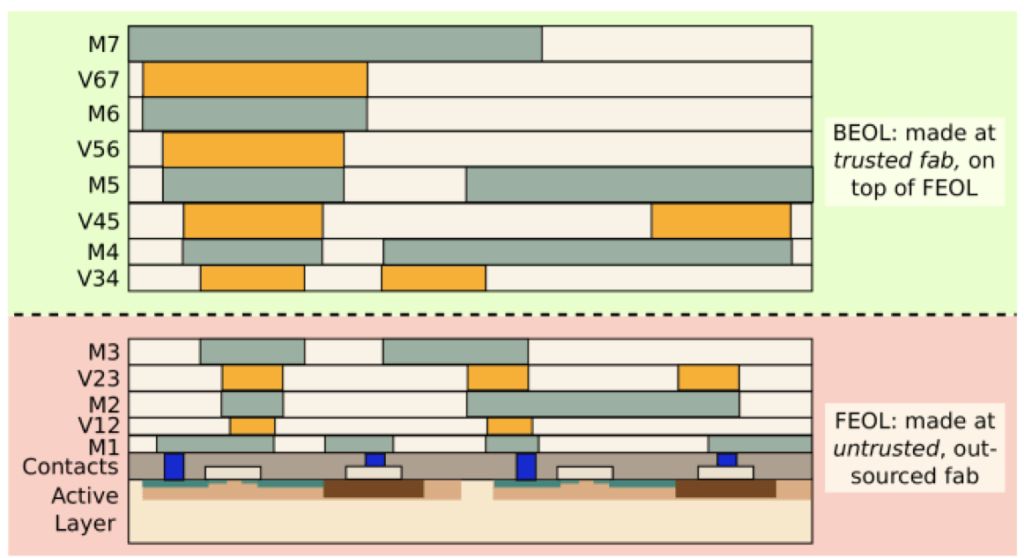
10: “Split manufacturing”
It addresses the fact that there is no “trusted foundry” in the US committed to developing processes below 14/12 nm. That’s why experts suggest separating front-end of line (FEOL) and back-end of line (BEOL) for design and manufacturing steps (Figure 3).
 9: Failure analysis and diagnostic strategies for new device types and structures:
 9: Failure analysis and diagnostic strategies for new device types and structures:
As new transistor types, memory technologies and materials are needed, their failure mechanisms need to be understood and test strategies developed to assure reliable functionality, even under harsh conditions, e.g. automotive.
8: Electromagnetic coupling – model extraction and analysis:
In addition to analyzing capacitive coupling (crosstalk) between nets, especially for longer lines and high-current power supply lines, inductive coupling needs to be analyzed and modeled to enable accurate simulations in the time and frequency domain.
7: Testing of resilient system designs – for cost-sensitive markets:
A fail-safe operation must be guaranteed for Level 5 Autonomous Vehicles and other – equally cost-sensitive – applications. Triple Modular Redundancy (TMR) and voting circuitry to disable a defective module, like deployed in airplanes today, is too costly.

6: Burn-in screening parameters for advanced process nodes:
The likely failure mechanisms for new materials, gate all around transistors, new memory technologies and other innovations need to be well understood, to define type and length of burn-in needed, to weed-out infant mortality.
5: Reliability analysis and aging:
Today’s FIT-rate (Failures in Time) calculations assume independent failure mechanisms, e.g. electromigration in a small piece of wire. But, how to combine all the individual FIT-rate numbers to get a meaningful total FIT-rate for Miles of wires and Billions of interconnects in a large SoC or SiP? Also, how to model device and interconnect aging mechanisms and predict their impact on reliability?
4: Electrical/thermal/mechanical analysis of complex systems:
Experts from several engineering disciplines are needed to work together to analyze, model and define multi-physics simulation methodologies, to capture these effects and their impact on system performance, reliability, and safety.
3: Improving designer productivity through higher levels of abstraction:
Yes, high-level languages simplify describing system functionality. But side-files are needed to implement e.g. clock spines and create power or voltage-islands. Also, for verifying an entire design, e.g. checking if the different abstraction levels are representing the same design intent and/or a large number of building blocks work together correctly, accurate models need to be created for every block and abstraction level. Considering that Engineering Change Orders (ECOs) are often required, it’s important that all these models and higher-level descriptions are being updated before the final design can be completely verified and accurately documented.
2: Utilization of “Digital Twin” models and simulation data:
The automotive industry, factory automation, suppliers of drones and surgery robots are a few examples of market segments that require full system digital twins for accurate and exhaustive simulation. Digital models for all building blocks (sensors, actuators, radar/lidar, antennas, GPS as well as electro-mechanical, chemical and fluid systems, …) need to be developed to prove that all building blocks work together well, and the entire system meets stringent safety standards.
1: “Pathfinding” methodologies for system partitioning, what-if analysis and early system optimization:
Improving designer productivity, minimizing iteration loops, optimizing system performance while minimizing power, unit cost and formfactor can be accomplished best very early in the design process. Planning and partitioning methodologies and user-friendly EDA tools need to be developed to enable meaningful pathfinding and fully utilize advanced manufacturing methods, equipment and materials capabilities.
While single-die designers focus today on optimizing performance, power and die area (=cost), the power, performance, area (PPA”) target is no longer sufficient to guarantee success. Dillinger suggested a much broader measure: Performance, power, area, cost, reliability and safety, (PPACRSS). (Hint for football fans: This acronym sounds like Green Bay “PACKERS”.
Dillinger’s Bonus Challenge
In addition to these ten points, Dillinger added, what he called a “bonus challenge” and mentioned a topic our industry already faces today and will, to a much greater extent, face in future: Managing statistical variations in chip/package/board design and fabrication. Another topic design, manufacturing and EDA experts need to address (and hopefully solve) together.
While some of the attending industry experts saw in all these challenges job security for many years to come, others looked quite concerned. To close on a very positive note, Dillinger listed many opportunities ahead for the electronics industry, such as: Autonomous driving, industrial and domestic robots, 5G networks, gigantic data centers, cloud computing for everyone as well as ML/AI algorithms and their many applications. Let’s hope that they’ll generate enough revenues and profits, to finance solving “Dillinger’s Top 10”!
I hope my brief summaries of “Dillinger’s Top Ten” and Joshi’s AI message encouraged you go to the MEPTEC Presentation Archive and listen to Dillinger’s and/or Joshi’s entire presentations and see all their slides.
Don’t forget to join us at the December MEPTEC event! December 11 Jan Vardaman will give her annual industry outlook titled: Advanced Packaging for 2020 and Beyond. Register here.
Thanks for reading….Herb


