


Part 1 of this advanced packaging (AP) article series focused on solving photoresist (PR) strip and under bump metallization (UBM) / redistribution layer (RDL) challenges. This article looks at AP trends from a lithography standpoint and proposes solutions to associated lithography challenges.
The need for advanced packaging solutions is greater than ever as the world continues to demand increased mobility, connectivity and data processing to provide higher performance and added functionality within ever-smaller form factors for today’s mobile devices. One advanced technique, fan-out wafer-level packaging (FOWLP), is a cost-effective solution and its adoption for manufacturing is expected to grow significantly over the next few years. While still a relatively new advanced packaging process in production, FOWLP continues to rapidly gain widespread adoption not only because of the smaller form factors but also due to its added advantages of true heterogeneous integration of a diversity of die types including tight pitch interconnects and passives with a short turnaround scalable manufacturing process.
From a lithography standpoint, FOWLP poses several challenges that need to be addressed for performance and yield. This article will review some of the lithography challenges and the solutions required to enable redistribution layer (RDL) line widths of 2µm or below using FOWLP.
Large depth of focus
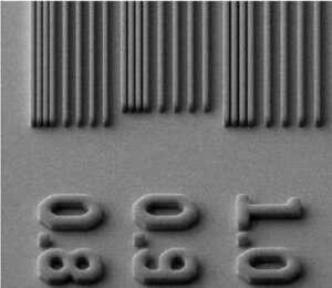
Future high-performance devices will require RDL line widths of 2 microns or below [1]. To image these smaller linewidths, the lithography process window must have a large depth of focus in order to accommodate the chip height variation after chip placement on the reconstituted wafer. The challenge lies in the fact that when the numerical aperture (NA) of the exposure tool is increased to image the smaller line sizes, this decreases the depth of focus. A viable solution has proved to be an adjustable, variable numerical aperture lens, coupled with a unique wafer topography mapping method for determining optimum focus position on a shot-by-shot basis. Utilizing these features, the lens can provide maximum depth-of-focus while maintaining the higher resolution performance required to achieve sub-2 micron and eventually sub-1.0-micron line resolution (Figure 1). The results are a system that enables high aspect ratio lithography and large depth of focus with the resolution required for next-generation FOWLP processes.
Full wafer mapping
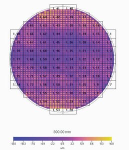
FOWLP wafers can have varied chip heights due to settling differences in the mold compound used to embed the chips [2]. To ensure efficiency and higher yields on reconstituted FOWLP wafers, it is important to be able to map the entire wafer topography to determine the best focus position for each exposure of the lithography system without impacting tool throughput. A lithography system that can provide a full wafer topography map enables the capability to optimize the focus position for each exposure (Figure 2). This can improve yield for FOWLP processes with smaller feature sizes by providing a full wafer topography map with ability to specify locations per field for extremely accurate shot-by-shot focusing.
Warped wafer processing
An additional challenge in FOWLP processing is the significant wafer warpage that must be accommodated by the lithography system. After the reconstituted FOWLP wafer has undergone the molding step, the wafer can have several millimeters of warpage due to process induced effects [3]. If a lithography system cannot efficiently process these highly warped wafers, both wafer and final device yields will be impacted. To address the high warpage requirements of FOWLP processes, a lithography tool must be capable of processing wafers with warpage up to 7mm. This requirement impacts how the robotic wafer transfer system, the wafer pre-aligner and especially the wafer chuck are designed. To meet specific FOWLP wafer requirements, these wafer handling capabilities must be carefully taken into consideration to optimize the process window and maximize chucked wafer flatness for sub-2 micron RDL lithography.
The technology team at Veeco is continuously developing solutions that improve our semiconductor manufacturing and process equipment to meet changing industry demands. The latest AP300 lithography tool for advanced packaging applications has a variable numerical aperture lens that can be optimized to maximize depth of focus while maintaining the higher resolution performance. Additionally, the AP300 stepper can be configured with an optical focus system that provides a full wafer topography map for optimizing the focus position for each exposure. These features, coupled with the capability for processing wafers with up to 7mm of warpage, provide a mature lithography solution for the challenging FOWLP processes required to manufacture high-performance next-generation devices.

Acknowledgments
The author, Doug Anberg, would like to thank his co-author, Warren Flack, Vice President of Worldwide Lithography Applications, Veeco Instruments Inc. for his contributions to this article.
References
[1] Flack, W. et. al., “One Micron Redistribution for Fan-Out Wafer Level Packaging”, Electronic Packaging Technology Conference, 2017.
[2] Hsieh, R. et. al., “Lithography Challenges and Considerations for Emerging Fan-Out Wafer-level Packaging Applications”, International Wafer-level Packaging Conference, 2009.
[3] Che, E., et. al., “Study of Process Induced Wafer Level Warpage of Fan-Out Wafer Level Packaging”, Electronic Components and Technology Conference, 2016.


