

![]()
Today’s electronic products present new challenges to product development teams. As a result, there is a constant push to improve product quality and design efficiency through the use of new design technologies. For example, system-scaling demands change as Moore’s law becomes increasingly difficult to maintain, thus driving growth of innovative PCB and packaging technologies such as:
- High-density interconnect and rigid-flex to enable more functions per unit area
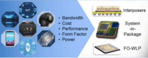
- Advanced packaging such as System-in-Package (SiP) and Fan-out Wafer Level Packaging (FOWLP) to enable the steady increase in design density.
 These innovative 2.5D and 3D “high-density” advanced packaging (HDAP) solutions not only disrupt traditional design methodologies and tools, they also disrupt the supply chain. With these disruptive technologies come new challenges as they employ silicon-like features and processes, or multi-substrate architectures to facilitate high-performance memory devices like High Bandwidth Memory and Hybrid Memory Cube HBM/HMC.
Package design methodologies and tools are, in fact, at an inflection point, one that is as significant as the transition from MCAD tools for lead frames to ECAD tools for Plastic Ball Grid Arrays (PBGAs). The entry of silicon foundries into the packaging supply chain further disrupts tools and methodologies with their application of silicon process design kits (PDKs) and verification processes to packaging. To draw an analogy to the IC world, these 2.5D and 3D HDAP technologies are in fact new “nodes” for packaging and as such require a new design and verification methodology.


