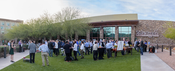
As part of the organizing committee, we believe this year’s IMAPS Device Packaging Conference really fulfilled what the announcement promised – the largest conference dedicated to the full spectrum of 3DIC and packaging, fan-out technologies and MEMS/sensors. We enjoyed 12% attendee growth over 2016, welcoming nearly 600 attendees from 20 countries, in addition to a 12th consecutive sold-out exhibition hall! In this short resume we would like to highlight just a few of the outstanding talks at the DPC presented by Ron Huemoeller, Amkor Technology; Lionel Rudant, CEA-LETI; Pascal Couderc, 3D-PLUS; Sitaram Arkalgud, XPERI (formerly Invensas); Markus Leitgeb, AT&S; and Maaike M. Visser Taklo, SINTEF.
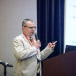
During the DPC opening session, the first speaker, Ron Huemoeller, corporate VP, worldwide R&D, Amkor Technology, Inc, presented “Heterogeneous Integration: Packaging the Future”. Ron explained how In the past few years, advanced packaging technologies have increased in complexity, transitioning from single to multi-die packaging, enabled by 3D integration, system-in-package (SiP), wafer-level packaging (WLP) and creative approaches for embedding dies. State-of-the-art heterogeneous integrated semiconductor packaging provides reduced form-factor, increased data transfer rate, improved signal integrity and memory bandwidth, all with reduced power and improved thermal performance.
Next, Lionel Rudant, CEA-LETI, introduced 5G networks and their impact on packaging roadmaps. 5G networks are expected to enable widespread internet of things (IoT) adoption by offering improvements like increased bandwidth and reduced latency. Microelectronics is now led by application-driven roadmaps, and new drivers for 5G systems are diverging IoT services that require flexibility and scalability from technology. Exploitation of innovative in-package integration of antennas was highlighted, together with the more widespread use of beamforming and multiple antennas. Rudant explained that there is a new complexity driving the technology roadmap since the transistor takes part of advanced system architectures where the software part is increasing.
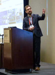
The first keynote speaker on Thursday was Sitaram Arkalgud from XPERI, who presented on “Trends in MEMS & Sensor Integration”. Sitaram is XPERI´s VP of 3D Applications. The combination of the keynote talk title and his job title shows clearly in which direction a great market track will be developing; a remarkable number of future MEMS and sensors products have a need for 3D Integration technologies! He focused on IoT as the third wave of MEMS proliferation, after automotive and mobile phones. “Smart objects” are a subset of IoT that show local intelligence and awareness.
We are in the phase of rapidly growing markets and increasing competition and we must reach for cost reduction, standardization, and increasing functionality and performance. A corresponding key is the simplification of processes and Sitaram´s talk focused correspondingly on wafer bonding processes. He discussed all relevant bonding schemes, including variants of glass-based and metal bonding – as thermocompression bonding (TCB) and solid-liquid interdiffusion (SLID), and compared production parameters with XPERI´s technologies called ZiBond and direct bond interconnect (DBI). Sitaram´s clear conclusion was that ZiBond and DBI, both low-temperature bonding technologies licensed to Fraunhofer Munich, offer sufficiently high bond strength for MEMS processing and 3D Integration of MEMS/IC products. The technologies are highly competitive as they result in process simplification, a particularly high throughput for a low-cost of ownership, and the interconnects are highly scalable. The scalability is critical for answering to the future needs of increased functionalities and performance of the bonded systems.
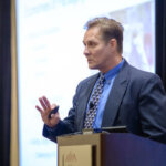
Thursday´s second keynote paper was presented by Markus Leitgeb from AT&S, who focused on embedding active and passives components into a large panel using PCB technologies. The PCB industry is well aware of the ongoing change in the electronic world and is developing innovative ways for supporting this trend of miniaturization and modularization of electronic devices, ending in an all-in-one-package.
Component embedding may not seem to be the latest break-through in PCB world; companies have worked on embedding in various shapes for more than 30 years (e.g. ECP® from AT&S). Besides the performance and form factor improvement (which are also offered by WLP technologies), embedding in laminate offers the economy of scale enabled by large panel format adopted in PCB production (18”x24” panel compared to 12” wafers).
Additionally, the PCB technology allows thick copper traces (up to 200µm) in the package, which is needed for current transport and advanced cooling of high power devices. For the two main product lines, SiP and system-in-board (SiB), Markus explained that only embedding in PCB can be used for both types due to large form factors needed in the SiB.
At the end of his presentation, Markus pointed out that PCB companies will have to transform from an interconnection provider to a full turnkey solution provider. Therefore, AT&S has started several activities in recent years to offer a high volume manufacturing capability and a product realization or even take over part of the supply chain.
 In the fan-out session, Pascal Couderc, 3D PLUS, described the company’s proprietary 3D technology named wire-free die-on-die (WDoDTM,), which is based on the stacking of known good rebuilt wafers using a fan-out wafer level package (FOWLP) process with only known good dies and PCBs with components. Interconnections are formed using a bus metal patterned with a laser. In this talk, two types of 3D modules developed in the frame of a study of implantable medical products (leadless pacemaker and neurostimulation were described).
These electronic 3D modules had several layers including PCB layers comprising components that cannot be processed with fan-out technology. Only layers with bare dies were processed using eWLB-based FOWLP technology. For one module, their so-called Flow 3.5 technology was used as an alternative technology to FOWLP. External sides of these modules could be populated with additional components interconnected with other sub-modules. They can also be solder balled in order to be reflowed as BGA components.

WDoD™ allowed smaller from-factor than other competitive 3D technologies like chip-on-chip and flex-folded PCB. You can read more details in the Knowledge Portal post here.
One of the last presentations in the track for Engineered Micro Systems/Devices was given by Maaike M. Visser Taklo from SINTEF on the topic of reliability of conductive adhesives. The results are part of a larger European project called Lab4MEMS II led by STMicroelectronics. The focus of the project is to reduce cost and improve manufacturability of assembly of optical MEMS, like mirrors and scanners. In that respect, SINTEF has studied the possibility of performing reliable flip-chip assembly of mirrors directly onto rigid-flex boards using conductive adhesives. A novel adhesive based on metal-coated polymers spheres, developed by Conpart, was found to have remarkable performance compared to a commercial reference material when exposed to hygrothermal aging. Exposure to humidity will be one of the key challenges of several future IoT devices as they will be placed all around us, also outdoors.
All the presentations and extended abstracts from the conference were published on April 4 and can be downloaded via www.imaps.org/devicepackaging/down/2017DPC_SECURED.zip
We invite you to enjoy reading the great papers of the three tracks of the conference:
- Interposers, 3DIC and Packaging
- Fan-Out, Wafer Level Packaging & Flip Chip
- Engineered Micro Systems/Devices
► Upcoming IMAPS events
Mark your calendars for the 14th International Conference and Exhibition on Device Packaging from March 5-8, 2018. Be sure to view details about all upcoming events at www.IMAPS.org, including the 50th International Symposium on Microelectronics in Raleigh, NC from October 9-12.
Editor’s Note: Peter Ramm, Gilles Poupon, Pascal Courderc, Markus Lietgeb, and Maaike M. Visser Taklo contributed to this article.