
“Growing photolithography equipment markets in advanced packaging, MEMS and LEDs are attracting new players; but they have to navigate complex roadmaps …” announces Yole Développement (Yole). The “More than Moore” market research and strategy consulting company confirms its leadership in the silicon manufacturing industry with its new technology & market report entitled “Photolithography Equipment & Materials for Advanced Packaging, MEMS and LED Applications”.
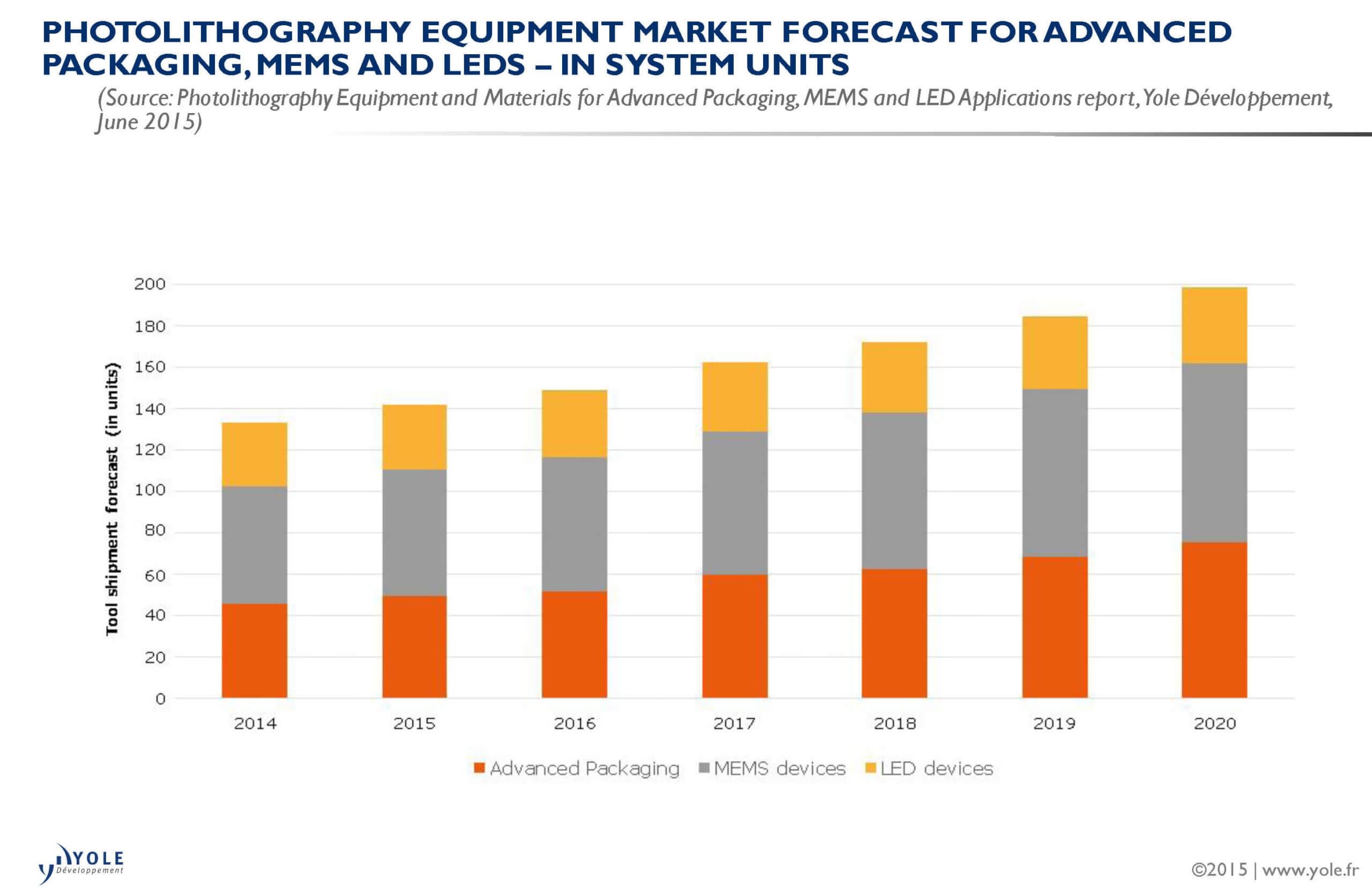
In this report, Yole’s analysts announce a projection system market for advanced packaging, MEMS and LEDs reaching more than US$150M in 2014. To perform this report, they interviewed leaders and outsiders of this market such as SUSS MicroTec, ASML, EV Group, Rudolph Technologies, USHIO … They analyzed their market positioning and their technical solutions.
Within a highly competitive and innovative environment, Yole’s analysis shows, at first glance, some similarities between “More Moore” and “More than Moore”. However the analysis is more complex…
“Photolithography Equipment & Materials for Advanced Packaging, MEMS and LED Applications” analysis provides a comprehensive overview of all the key lithography technologies used in advanced packaging, MEMS and LED applications and benchmarks them in terms of feature requirements. Yole’s analysts provide examples of lithography process steps for these applications. In parallel, Yole’s report describes associated technological breakthroughs and manufacturing process. More insights are included on specific lithography equipment tools for advanced packaging, MEMS and LED devices.
The semiconductor industry is very often identified by its “More Moore” players, driven by technology downscaling and cost reduction. There is one clear leader supplying photolithography tools to the “More Moore” industry: ASML, based in The Netherlands. The company proposes lithography equipment with $10M unit price and incredible optics, mechanics and precision stage in order to reach sub 20nm precision (Latest announcement from ASML, April 2015). ASML is followed by two Japanese outsiders, Nikon and Canon.
“Providing this market with photolithography equipment is highly complex and there are gigantic barriers to market entry” asserts Claire Troadec, Technology & Market Analyst, Semiconductor Manufacturing at Yole. Enormous R&D investments are required as the key features to print shrink ever further. Also, the tolerances specified are very aggressive and thus equipment complexity keeps on increasing.
In the “More than Moore” industry the Holy Grail isn’t downscaling any more – it is adding functionality: according to Yole’s analysis, there are two clear leaders today: SUSS MicroTec (Latest order: lithography tools from TDK, Feb. 2015) in the MEMS and sensors industry, and Ultratech in the advanced packaging industry. Both players are closely followed by the following outsiders, EV Group, Rudolph Technologies and USHIO.
“But the similarities between both worlds, are only superficial”, comments Amandine Pizzagalli, Technology & Market Analyst, Advanced Packaging & Semiconductor Manufacturing at Yole. “Indeed market entry barrier is much lower in the “More than Moore” market. Equipment in the Advanced Packaging, MEMS and LEDs industries is less complex but customer adoption needs are higher, which leads to a much broader photolithography landscape”, she adds.

The photolithography market structure for these three industries is very different compared to the “More Moore”, or mainstream semiconductor, industry. New entrants can penetrate these markets with a good knowledge of the technological building blocks. But the key to success is to adapt the equipment to the specific customer’s needs. That means that these markets are complex to develop and that they take a long time to penetrate.
To develop their knowledge and expand their range of products, some players entered through acquisition. Rudolph Technologies acquired Azores Corp. in 2012 to enter the advanced packaging photolithography equipment arena. Also in 2012, SUSS MicroTec acquired Tamarack Scientific Co. Inc. to enlarge its semiconductor back end photolithography equipment market.
Others like Orbotech, which acquired a leading MEMS and advanced packaging company, SPTS, is today only present in substrate and PCB direct imaging.
In this report, competition trends are carefully analyzed and presented as a competitive landscape and competitive analysis of the major equipment and materials suppliers involved in Advanced Packaging, MEMS and LED applications. Finally, a section is also dedicated to disruptive technologies such as LDI, laser ablation and nanoimprint lithography, which could reshape the lithography landscape in the future. Yole describes possible reshaping scenarios, including acquisitions, mergers, and joint ventures, along with their anticipated impact on the global photolithography market
A detailed description of the lithography equipment and materials report is available on www.i-micronews.com, manufacturing section.
Source: www.yole.fr