
Last Tuesday, April 7, was another important day for Silicon Valley. TSMC 2015 Technology Symposium celebrated 21 years of holding this annual event to update TSMC’s loyal customers and win new ones.
Rick Cassidy, President TSMC North America, opened the symposium with a long list of impressive numbers about TSMC and put them into context with our Semiconductor industry. For example: TSMC shipped 5.1M 12” equivalent wafers, for 5066 different products in 2014. In Q4 North America accounted for 74% of TSMC’s worldwide revenues. TSMC plans CapEx of USD 11.5 to 12B for 2015 and also will invests more than USD 2B in R & D.
Dr. Mark Liu, President and CoCEO of TSMC, added more facts to Cassidy’s numbers, such as: TSMC employs 4,700 R&D engineers, runs 11 wafer fabs, to service currently 456 active customers, and adds one more customer every week. Talking about customers: I liked very much that Avago’s President and CEO, Hock E. Tan, and Illumina’s SVP, Bob Ragusa, had the opportunity to share their work and experience with TSMC with the audience. Their brief presentations added the customer perspective to the long list of TSMC presenters and their messages. In addition, like in previous years, many of TSMC’s EcoSystem partners were exhibiting their strengths and added further credibility to the capabilities of the world’s largest wafer foundry.
TSMC’s technology leadership was the next topic Dr. Liu covered in his talk: He projected more than 50 tape-outs for 16 FF+ technology in 2015 and mentioned that more than 10 customers are already working with TSMC’s 10nm process, with risk production planned for 4Q 2015. Both 16 FF+ and 10nm technologies and the very short production ramp-up times for new processes show that TSMC can respond quickly to their high-volume customers’ demand for continuing improvements of performance, power, and area (PPA).
Dr. Y.J. Mii, VP R&D, presented further technology and production facts: 16 FF+ technology yields are now close to the 20nm production yields and 10nm offers an area scaling factor of 0.52 – compared to 16nm. About TSMC’s EUV cooperation with ASML: Dr. Mii stated that source power has been increases to 90 Watts and projected to grow to 150W in 2015. TSMC is also working on multi-beam technology, inverse litho, and direct self assembly (DSA) to reach < 24nm for trench/line spacing. As announced last year, TSMC’s work on their IoT enabling ultra-low power processes, with 55, 40 and 28nm feature sizes, continues. In contrast, TSMC also develops processes for automotive and industrial applications to switch up to 70V. Finally, Dr. Mii also talked about TSMC’s work on heterogeneous and multi-die solution like stacked CMOS sensors, monolithic logic, and MEMS integration. He confirmed that chip-on-wafer-on-substrate (CoWoS) technology is production-proven and offers now interposers with up to 32 x 36mm size and fine-pitch routing for high-end multi-die designs, like Xilinx’ FPGAs. To serve market needs for lower cost and less demanding (RDL pitch 10/10μm) applications, TSMC will ramp their wafer-level InFO packaging technology in 2Q 2016 and offer an InFO PoP combination as well.
The next speaker, Dr. Cliff Hou, VP R&D/Design & Technology Platform, presented TSMC’s design solutions to enable customers to fully utilize TSMC’s process technologies and manufacturing capabilities. In addition to the many requests he gets in his TSMC role as GUC board member, Dr. Hou also hears from GUC’s IC designers and EDA tools users about the latest challenges and requirements. He showed a series of tables, detailing the exact 16nm and 10nm qualification status of EDA tools from Ansys, Cadence, Mentor, and Synsopsys. Dr. Hou also described the ongoing work to demonstrate the value of TSMC’s ultra-low power technologies by the end of this year and in 2016. ARM and Dolphin are TSMC’s partners for 55nm reference designs, Synopsys for 40nm and Imagination is working with TSMC on an ultra-low power 28nm design.
Dr. Hou kept me in suspense until the last few minutes of his talk. Finally, he outlined his team’s commitment to develop a CoWoS reference design flow by 3Q2015 that will consider the impact of bumping, power- and signal integrity challenges, thermal management as well as recommend DFT strategies.
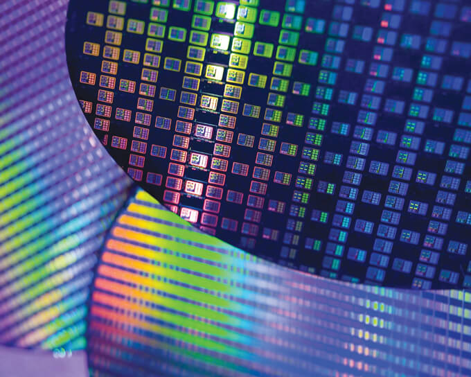
The morning session would have been incomplete without addressing TSMC’s manufacturing facilities: Fab 12 in Hsinchu, Fab 14 in Tainan, Fab 15 in Taichung and several sites in other locations. JK Wang, VP operations for TSMC’s 300mm wafer fabs, described the roles of their 12” GigaFabs (# 12, 14, 15), the 8” wafer fabs, the roles of back-end fabs BP 1 and BP 2 as well as the planned BP 3. I also learned that TSMC now operates 5 mask shops and that TSMC’s fabs are not “only” highly automated but also intelligent – they respond to deviations in a pre-defined, automated way – to get back to the full spec compliance quickly.
After great networking during lunch and in the exhibition area, Dr. BJ Woo, VP business development, started the afternoon. He talked about the growth opportunities IoT will offer IDMs, fab-lite and fabless IC vendors and of course TSMC. Dr. Woo showed how prepared TSMC is to meet the need for higher performance in data centers and local IoT hub as well as how TSMC’s ultra-low power technologies, with supply voltages below 0.6V for both logic and memory, will assure long battery life for IoT peripheral.

Suk Lee, Senior Director Design Infrastructure Marketing, showed in-depth information to complement the data Dr. Hou showed in the morning. Lee also talked more about TSMC’s currently 24 EDA and 31 IP partners and their 8600 IP titles TSMC has verified, using Atrenta’s Spyglass tool. Lee commented on the completed 16nm and ongoing 10nm qualification efforts with Synopsys, Cadence, Mentor, Atoptech and Silvaco/Invarian design tools. He explained the CoWoS characterization reports, and talked about the TSMC reference flows for CoWoS and InFO. These flows will include cross-dice STA, integrated DFM and other important capabilities for the low-cost InFO wafer-level packaging technology.
After a short networking break George Liu, Senior Director Business Development for Sensors and Displays, presented TSMC’s specialty technologies in support of rapidly growing markets, such as IoT and other applications. Liu gave examples how IoT makes cities smarter: Amsterdam, Barcelona, Copenhagen, Rio, Santander and Seoul (all non-U.S.?) deploy sensors to perform their services more efficiently. He also talked about smart homes, wearables, energy harvesting, MEMS and the higher bandwidth the new 5G technology will offer to enable many more IoT applications. That’s a wide range of new opportunities for innovative semiconductor companies to conquer, together with TSMC. Liu also highlighted the need for precision analog, power management circuits, hardware security (e.g. OTP), image sensors and other applications. He hinted that they’ll be best addressed with heterogeneous integration, using interposers or vertical dice stacking (3D-ICs).
Dr. Marvin Liao, Senior Director Backend Technology and Services, focused his 30 minutes on packaging technology – the “Backend” from a wafer foundry’s perspective. He explained that mobile computing represents 60% of TSMC’s business and demands many improvements: Performance vs power, bandwidth, wiring pitch, thermal performance, smaller and thinner packages, shorter time to market and of course lower cost. Liao mentioned that for the 10nm node TSMC is developing copper bump pitches from 80 down to 40μm, larger interposer sizes of up to 650 mm² (= 1 square inch) and WLCSP for up to 800 I/Os. He explained that TSMC’s InFO technology will allow replacing the costly substrate in flip chips with finer pitch and lower inductance interposers. For the proven CoWoS technology, e.g. at Xilinx, Liao mentioned an impressive yield number: 96%. He also talked about Nvidia’s latest graphics design: 4 HBM memory cubes from SK hynix surround the GPU on an interposer and offer 1TB/sec bandwidth – 3 times the previous design’s bandwidth, at the same power budget. Last, but not at all least, Liao emphasized in great length, the importance of partnerships and a well-functioning ecosystem. TSMC is cooperating with the four big assembly houses (ASE, Amkor, SPIL and STATSChipPAC, which got new owners recently), the suppliers of memory cubes (Samsung, Micron, SK hynix), substrate suppliers (Ibiden, Unimicron) and others.
In summary, a very productive day, filled with impressive presentations and 1-on-1 discussion from across the entire semiconductor ecosystem. I look forward to TSMC’s 2016 Symposium and the progress TSMC is positioned to make in the coming year. ~ Herb
P.S.: It’s not to late to hear these presentations in person. TSMC’s 2015 Technology Symposium takes place tomorrow, April 14, 2015 in Boston MA, and on the April 16th in Austin TX.


