

It’s been a long time coming, but Kulicke & Soffa has seen the writing on the wall, and it reads: “2.5D and 3D IC assembly is a hot market.” Why else would the wire-bond giant invest in developing a thermocompression chip-to-substrate (C2S) bonder for high-volume 2.5D and 3D IC die stacking processes?
The company first dipped its toes in the die bonding market when it acquired Alphasem back in 2006, seeing a natural growth path for K&S; but since then have been relatively quiet about die bonding activities. Earlier this month at SEMICON Taiwan, however, K&S unveiled the APAMA C2S thermo-compression bonder, which targets die stacking based on through silicon vias (TSVs) as the method of interconnect, rather than wire bonds.
When a supplier that targets high volume manufacturing (HVM) gets in the game to support a technology that competes directly with its established core competency, I have questions. So I contacted the company and was connected with Tong Liang Cheam, Vice President, Strategic Marketing & Business Development for K&S, who filled me in on some of the details and motivations.
Cheam explained that advanced packaging has long been a focus of growth for K&S. As the demand for performance, bandwidth, and power consumption in many mobile applications increases, they see advanced packaging gaining momentum for potentially high growth. “Advanced Packaging comes in many forms, and entering into the 2.5D and 3D IC market is part of our overall advanced packaging strategy,” he explained.
However, Cheam doesn’t really see 2.5D and 3D as a threat to the wire bond industry. “We are anticipating only the high performance applications moving to 2.5D and 3D IC,” he explained. “Cost is still a barrier, and wire bonding is still the most cost effective solution. It is very flexible too.”
It’s well known that C2S or chip-to-wafer (C2W) stacking is tricky business when TSVs are involved. It requires higher placement accuracy, not only along X and Y axes, but also parallelism between chips. So far, the only company to achieve post-bond accuracy below 0.5µm has been French device bonder manufacturer, S.E.T. However they have had to sacrifice speed to do this, which is necessary for HVM applications. SET tools have been widely used by research centers in developing 3D IC processes. While SET’s tool is a thermocompression bonder, it’s not suited to HVM. Amicra Microtechnologies, based in Germany, claims to have achieved placement accuracies of +/-2.5µm with a 3 second cycle time. While considered suitable for HVM, Amicra’s tool does not perform thermocompression bonding, but rather eutectic bonding. “We don’t consider SET and Amicra as our competitors,” noted Cheam.
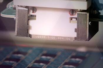
Cheam agrees that placement accuracy/speed is a challenge to be overcome for HVM die stacking, but thinks K&S has made headway. “We have managed to get to a reasonably high UPH with high accuracy due to some innovative designs,” he said.”Our post-bond accuracy is at 2µm (3 sigma). The UPH is dependent on the process, and is difficult to give a number without a specific process. However, our sprint UPH is 3000. Our heating and cooling rate of 200 deg C/sec and 100 deg C/sec respectively are industry leading and are fully programmable to enable maximum throughput.” According to the company website, the key to these designs is a direct-drive Z-axis bond head with precise motion control for accurate placement with both low and high bond force.

“We worked very closely with some alpha and beta customers to develop this tool,” noted Cheam. “We already shipped a few machines to our alpha and beta customers.”
What’s next for K&S in this space? According to Cheam, the APAMA C2S is the first of the thermo-compression bonders in the APAMA series of products from K&S. “We believe this is a growth area and are committed to it. We have more than 120 development engineers dedicated to advanced packaging,” he said.
As low volume production of memory stacks is underway, Cheam says K&S is anticipating HVM production in the 2016/2017 timeframe, based on analyst predictions. And when it comes, K&S will be ready. ~ F.v.T


