

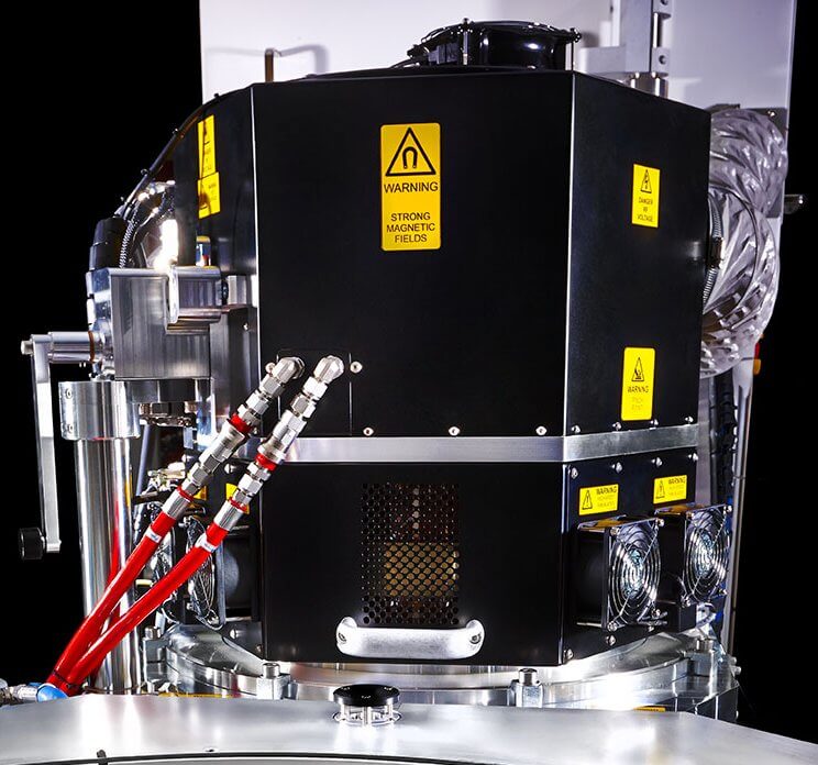
 Newport, United Kingdom, 22 May, 2014 – SPTS Technologies, a supplier of advanced wafer processing solutions for the global semiconductor industry and related markets, today announced the launch of its Rapier XE system for 300mm wafer silicon etch processing. The new module offers significant advantages over competing systems as well as improved etch rate over the 1st generation Rapier in applications where “blanket” etching or removing a large exposed area of silicon is required, such as via reveal processing.
In 3D-IC applications, via reveal processing occurs after the through silicon vias (TSVs) are formed, to prepare the vias for redistribution metallization. After completion of front-side wafer processing, the wafer is temporarily bonded, face down, onto a carrier wafer. The active silicon is then ground typically to within 5-10 μm of the TSV nodes. The silicon is then dry etched in a process that ‘reveals’ the vias to a step height typically in the range 2-5µm. To maximize yield, it is critical that all vias are revealed to a uniform height, which can be extremely challenging if the incoming wafer thickness varies across a wafer or from one wafer to the next. In the 1st generation Rapier and now the new Rapier XE system, issues of wafer-to-wafer silicon thickness variation is overcome with the use of the ReVia™ endpoint system.
Dave Thomas, SPTS’ marketing director for etch products, explained: “While the dual-source design of our 1st generation Rapier proved useful for tailoring the cross-wafer etch profile, coupled with our in-situ ReViaTM endpoint system to deal with wafer-to-wafer non-uniformities, we saw the need to improve etch rates for more cost-effective high-volume production. Our engineering and R&D teams worked closely together to develop a solution that delivers a blanket silicon etch rate on 300mm wafers 3 to 4 times faster than competing dry etch systems, with a cross-wafer uniformity of ≤+/- 3%. This enhanced design is also available to existing Rapier customers as an upgrade which can be retrofitted in the field.”
Kevin Crofton, president and COO of SPTS added, “With this new etch product, and our other processes like low temperature PECVD, we believe we offer our production customers the best throughput and process control for 300mm via reveal processing currently available on the market. We continue to be committed to helping our customers improve throughputs and device yields while reducing costs, wherever possible, to remain competitive.”
SPTS will be showcasing its range of etch, deposition and thermal processing as well as advanced packaging solutions at ECTC 2014 at Walt Disney World Swan and Dolphin Resort, 27-30 May, 2014. To learn more, email enquiries@spts.com to arrange a meeting or just visit us on Booth #218 in the Technology Corner.

About SPTS Technologies
SPTS Technologies (a Bridgepoint portfolio company) designs, manufactures, sells, and supports etch, PVD, CVD and thermal wafer processing solutions for the MEMS, advanced packaging, LEDs, high speed RF on GaAs, and power management device markets. With manufacturing facilities in Newport, Wales, Allentown, Pennsylvania, and San Jose, California, the company operates across 19 countries in Europe, North America and Asia-Pacific. For more information about SPTS Technologies, please visit www.spts.com
Company Contact: Destanie Clarke, Destanie.Clarke@spts.com


