What can we expect out of 2.5 and 3D TSV Integration? What are the three leading-edge R&D institutes in 2.5 and 3D TSV investigating?
On November 18, SEMI offered a webinar entitled “3D TSV without Limits.” Francoise von Trapp of 3D InCites moderated the webinar which featured Eric Beyne, director of 3D System Integration program at imec, Herve Ribot, head of 3D at CEA-LETI and Juergen Wolf, department head of HDI WLP/ASSID at Fraunhofer-IZM. Beyne, Ribot and Wolf shared insights with the participants and presented introductions to the topics they will present at the European 3D TSV Summit (20-22 January in Grenoble).
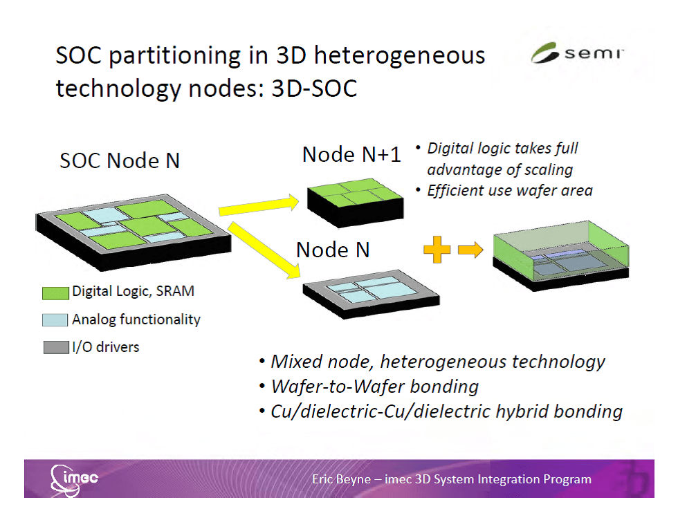
Eric Beyne of imec focused his talk on the applications drivers to justify the use of TSV and consequently enable 2.5 and 3D IC integration. Beyne started by presenting the now well identified application “sweet spots” for 3D TSV: wide I/O memory directly stacked on top of a processor, 3D SoC composed of two heterogeneous partitioned tiers with high density interconnect in between, and finally the multi die memory stack.
For all these applications, imec is proposing to use a high-density via middle TSV with a process of reference of 5µm diameter, 50µm deep and aspect ratio of 10. So still with the ambition to reduce the TSV cost and enable higher density interconnect, imec investigates higher aspect ratio TSV up to 17, trying to solve the barrier and seed deposition challenges and by keeping in mind the constraints related to advanced CMOS nodes.
Beyne insisted that TSV cost is only a portion of the 3D total cost. In fact, all post TSV process steps such wafer thinning, TSV reveal, µbumping, carrier bonding/debonding, and the stacking process itself up to final assembling contribute to the global solution cost. To lower the overall cost of these various process steps, imec is investigating different paths — for instance an alternative backside wafer via reveal process or the possibility of using the TSV tip itself as a Cu post.
For a longer term perspective than the interposer approach that might be required in case of thermal constraint, Beyne mentioned the possibility — for overall cost effectiveness reasons — of building a 3D SoC with high-density TSV instead of building a traditional monolithic 2D SoC that does not always take full benefit of the most advanced technologies. Porting only the scaling functions to the next technology node and keeping some IPs and functions in a more mature process might reduce the cost of next-generation product.
Concluding his talk, Beyne announced that he will deliver a more detailed presentation on cost analysis of the different 2.5 and 3D configurations at the European 3D TSV Summit 2014 organized by SEMI in Grenoble (France).
Herve Ribot from CEA-LETI discussed 3D and Photonics convergence for high-bandwidth chip-to-chip communication. Ribot began his presentation by noting that it is time to consider optics as a way to connect ICs inside electronics devices such as high-performance computers, mainly for energy efficiency reasons.
Referring to previous 3D achievements by LETI with ST-Ericsson, Ribot underlined the benefits of TSV as a way to drastically reduce power consumption. Still, the benefit of TSV compared to a traditional connection is impacted by the losses in the long horizontal copper redistribution lines. So the approach investigated by LETI for high-performance computing is to combine electronics for vertical and short horizontal connections and photonics for longer horizontal connections. Pragmatically that means stacking ICs and optic components on top of a silicon hybridized photonics interposer. Doing so, high attenuation and power consumption in narrow copper redistribution lines can be overcome.
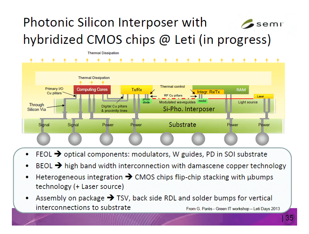
The work described is currently under design and the silicon processing phase is planned to start in early 2014. Additional details about this major project will be shared by Ribot during his presentation at the European 3D TSV Summit in a session focusing on the Applications & Products. His presentation will also contain information about the improvements TSV can bring to imaging products.

Jürgen Wolf from Fraunhofer IZM presented the Fraunhofer approach to 3D Wafer Level System Integration. He insisted on 3D System Integration being a global package containing not only the technology aspect but as well design and reliability parts. Wolf introduced the Fraunhofer cluster for 3D Integration that gathers five Fraunhofer Institutes with each one having his core competencies around these design, technology and reliability domains.
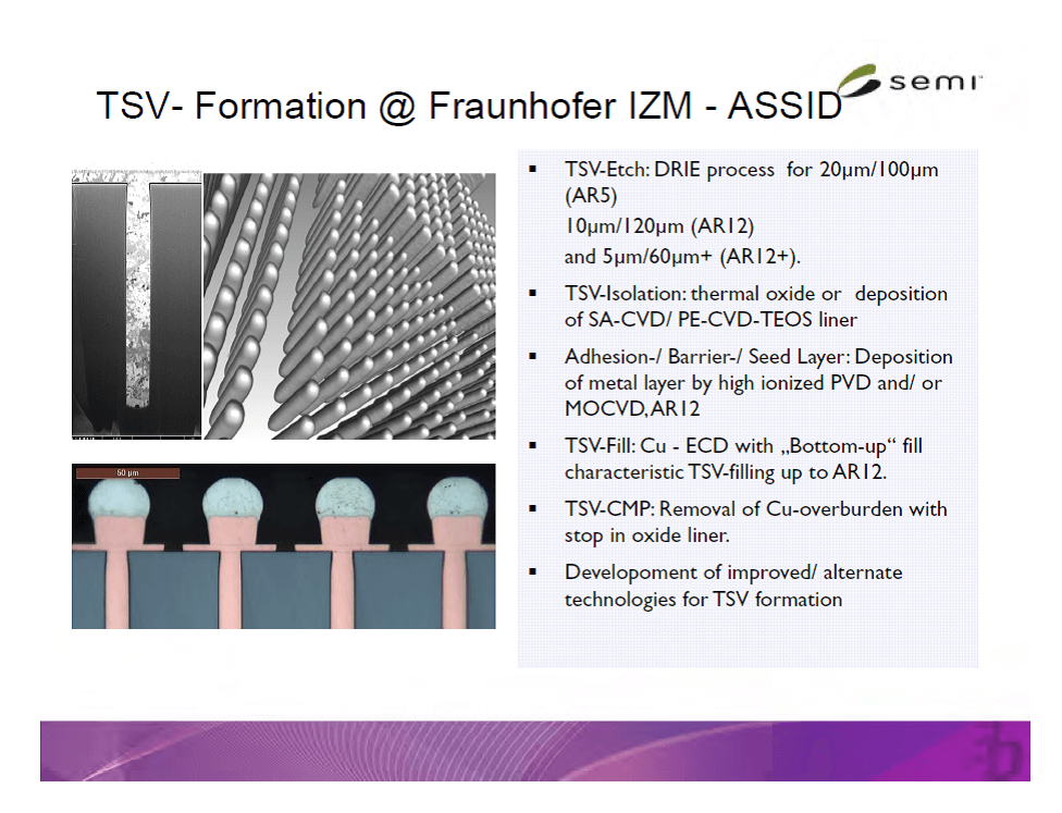
Focusing naturally on technology as a representative of Fraunhofer IZM, Wolf presented their technology toolbox. He described IZM capabilities around the TSV module from etching, isolation, barrier/seed, filling and overburden copper removal.
Regarding wafer bonding and debonding from carrier, Wolf talked about specific developments from Fraunhofer-IZM to reduce the cost of this process step and improve the throughput. Discussing die-to-die interconnect, he mentioned different technologies but said copper tin silver (CuSnAg) was the mainstream solution. Wolf illustrated his presentations with various prototypes achieved in Fraunhofer-IZM with a focus on MEMS and sensor applications
Wolf will delve deeper into the Fraunhofer-IZM approach at the European 3D TSV Summit in a presentation entitled “3D Technology as a Holistic Approach: Quo Vadis.”
A recording of the webinar is available here.
For a complete status on the 2.5 and 3D TSV situation, hear from experts and executives from all over the world at the European 3D TSV Summit (January 20-22) in Grenoble, France. Registration is now open. ~ YG
This post was reposted with permission from SEMI. It first appeared on December 3, 2013 in the SEMI Global Update.