
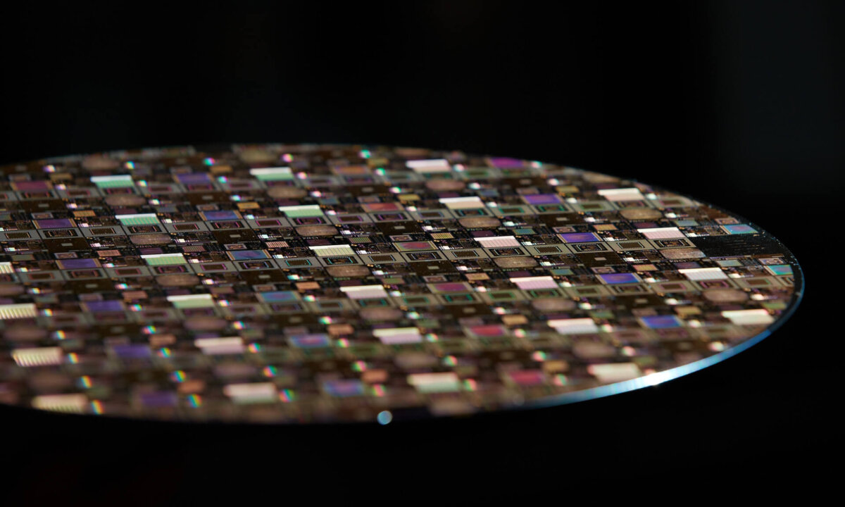
A few months ago, Juergen Wolf, director of the 3D program at Fraunhofer IZM-ASSID, shared with me a beautifully photographed image of a 2.5D multi-project interposer wafer. I’ve been saving it for the next time I interviewed him. So it was the first thing I asked him about when I met up with him at the Silicon Saxony booth at SEMICON West.
 It’s a second-generation 2.5D passive interposer test wafer for qualifying processors, materials and designs, he explained. Specifically, the 16 sub-projects on the reticle include Wide I/O DRAM design study, inductive arrays, TSV capacitor arrays, TSV daisy chains, and interconnect design studies.
But what Wolf wanted to update me about more was a new collaborative effort beyond what exists within Fraunhofer IZM ASSID itself, that integrates five Fraunhofer institutes to further the development of 3D integration. The Fraunhofer 3D Integration Cluster, as it’s called, was established to cope with the increasing complexity of 3D integration. The idea is for the participating institutes to cluster their competencies in a network to cover a broad spectrum of topics related to 3D integration, including design, technology, and reliability.
All located in Saxony, the five participating “Fraunhofers” include the Institute for Reliability and Microintegration IZM; the institute for Electronic Nano Systems ENAS; the institute for Integrated Circuits IIS, Design Automation Division EAS; the
=Institute for Nondestructive Testing Dresden branch (IZFP-D); and Institute for Photonic Microsystems IPMS.
Prior to organizing the cluster, all the institutes worked with customers individually. The 3D Integration Cluster was established is to exploit the synergy between all the parnters, explained Wolf. “The purpose is to provide a ‘one hand’ solution to the customer with a single access point,” he said. 3D integration involves more than just the technology. It requires collaboration between technology, failure analysis, design, simulation, modeling, etc. Each of the institutes specializes in a different area but come together to focus on 3D integration.
IZM-ASSID has always been the technology provider focused on technology transfer to customers such as GLOBALFOUNDRIES, NXP and Infineon. As such, IZM-ASSID provides qualified services and technology for 300mm chip scale packages, interposers, TSVs, TSV via-mid/via-last integration, bumping, and interconnect formation. Internally, it has established materials and supplier partners (Applied Materials, Oerlikon, SPTS, EV Group, SUSS MicroTech, Brewer Science, and TMAT.)

Wolf also updated me on new partner activities. The’ve recently teamed with single wet wafer equipment manufacturer, SEMSYSCO, headquartered in Villach, Austria, to develop wet etch and TSV clean processes for 3D ICs. To develop TSV measurement processes, they’re teaming with Israel-based metrology tool manufacturer, Camtek. And for TSV depth measurement, they’ve partnered with ESYS GmbH, in Berlin. Additionally, they are working with material supplier partners to develop new electrolyte materials for electro-deposition, photoresists, and dielectric.
With all of these activities underway, I expect to here more next time we meet. ~ F.v.T.


