

Don’t let the skeptics fool you, contrary to popular belief, the 3D test community has been hard at work on solutions for overcoming 3D test challenges. I am attending The Fourth IEEE International Workshop on testing 3D Stacked ICs (3D Test Workshop for short) at the Disneyland Hotel in Anaheim, and its clear that at least here, solving 3D challenges is at the top of everyone’s to-do list. The event kicked off on the afternoon of Thursday, September 12, 2013, directly on the heels of ITC Test Week. As is customary, the workshop followed a more casual format than ITC, and began with a Keynote by Nicholas Ilyadis, VP and CTO, Broadcom Infrastructure and Networking, who talked about 3D solutions in the coming age of terabit computing.
To provide a framework for Broadcom’s growing interest in 3D integration technologies, Illyadis talked about the data usage growth and the Internet of Things. “Computing has become just like electricity. Plug it in and its there. It’s become a utility.” he noted.
To accommodate this need, Broadcom has its StrataXGS which has 4B transistors. Illyadis called it “the test engineer’s nightmare.” The company’s new multicore processor features 5B transistors. But this still won’t meet the growing need for more data. The conclusion? “We have to go vertical. That’s why I’m speaking at a 3D test conference.” he said.
Ilyadis pointed out various system challenges faced by Broadcom that may be solved with 3D solutions, such as switching chips and network I/O bandwidth; port fan-out is a big challenge, and on-chip memory is taking up more chip area, he said.
He also shared examples of intriguing 3D solutions being developed by Cisco Systems and Lincoln Labs to solve the system challenges he outlined. Cisco System renditions involves a combination of multi-die, 2.5D and 3D integration schemes.
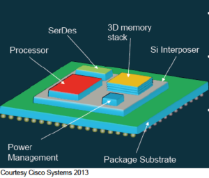
The schematic he shared displayed a Si interposer with a microprocessor, SerDes, 3D memory stack, and power management module, all mounted on a package substrate. Lincoln Labs is also exploiting different heterogeneous process technologies. While he couldn’t disclose what type of 3D device Broadcom would come out with first, he did say 3D is on the roadmap for next 2-3 years. Why not sooner? “We’re still pushing reticle size,” he said. “We haven’t run out of gas yet but its close.”
Ilyadis concluded his talk by identifying some test challenges that need to be addressed including known good die (KGD), test as you grow, built-in-self-test (BIST) and scan solutions, and fault isolations. “I’ve always had religion for BIST,” he commented, “especially when you lose visibility in stacks, BIST is going to be great.”
This conclusion was a great segue into the afternoon panel discussion, which was focused on “Requirements for 3D Volume Production Testing.” Panelists included Samam Adham, from TSMC Canada; Amer Cassier, Qualcomm; Manuel d’Abreu SanDisk; Amit Majumder, Xilinx; and Mike Ricchetti, AMD; and was moderated by Bill Eklow, Cisco Systems. Eklow set the stage by asking the panel to address what we need to do when 3D IC is a mainstream technology.
With the exception of D’Abreu, who focused his talk mainly on SanDisks’ goal of delivering high volumes of low cost Flash memory and the company’s work in 3D NAND, the panelists offered consensus opinions on challenges. For SanDisk, D’Abreu said TSVs are not an option because of the ultra-thinness of the wafers being stacked. The company has achieved 8-16 die stacks using wirebond, but is beginning the transition 3D NAND, which has different test requirements all together, focused on the silicon rather than the package. “3D ICs is not the end-game for SanDisk,” noted D’Abreu. “Our goal is to get product out in high volume at the lowest cost per gigabyte. 3D is just one way of doing it. There are more options than just TSVs.”

There was lots of discussion around the importance of KGD, known good stacks (KGS), the economics of test, when to test, when not to test, and the need for solutions to probe micro-bumps without creating faults in the process. Adham noted that 2.5D/3D IC test has the added complication of dealing with different suppliers of wafer and die. Inspection of incoming die for high yield is very important. “You can achieve high volume manufacturing if you can constrain the incoming die.” He estimates TSMC’s die yield at 99.999%. However, it was noted by the panel that final stack yield is what’s important, and consensus among the panelists was that it is coming in around 93-95% yield, which indicates failures happen during the stacking process.
Cassier talked more of about post-stacking failures, pointing to the thin wafer handling and faults caused by probing the delicate structures. His solution to test economics was to “think traditional flow” with multi-site probing on C4 bumps, but than only sampling on microbumps and thin wafer probe on film frame. Adham referenced a work-around for probe challenges that involves creating sacrificial bond pads that are only used for probing to check for KGD and otherwise have no purpose in the stack. This could help prevent damaging the microbumps needed for interconnect.
According to Majumdar, as successful as Xilinx has been, it’s been “very hard learning the whole process.” he said good economics of 3D stacking was “learned on someone else’s back” referencing Xilinx and TSMC. And what they’ve learned with regard to test, is that if the margins are high, you can test whenever you want and just throw away the bad parts.
“The reality is, KGD requires us to invest in test and test time. For us it should be 4D test because it requires a lot of time,” he joked. He also said that KDG isn’t good enough, we need to pay attention to wafer sort, and go with known good bin (KGB). Mixing parts from multiple bins in the same package results in revenue loss. Richetti agreed, referencing what he called the die-to-ship ratio as being the most critical. You need to have a cost-effective model for product you’re building, noted RIchetti. His prescription for test success: partial assembly test, and TSV redundancy. “Thats what you have to rely on to make it work.”
The big picture always comes back to collaboration. “If we want 3D to succeed, we have to get it out of the one or two companies behind it.” noted Majumdar, “We need to get everyone involved and have multiple suppliers. We need consortia to fund other companies. Otherwise its not going to be an industry solution but will die after 5 years.” And that would truly be a sad day for all of us. ~ F.v.T.


Francoise wrote: “Adham noted that 2.5D/3D IC test has the added complication of dealing with different suppliers of wafer and die. Inspection of incoming die for high yield is very important. “You can achieve high volume manufacturing if you can constrain the incoming die.” He estimates TSMC’s die yield at 99.999%. However, it was noted by the panel that final stack yield is what’s important, and consensus among the panelists was that it is coming in around 93-95% yield, which indicates failures happen during the stacking process.”
The way I understood the discussion is that single-TSV yield is at “five nines” (=99.999%). This has to be multiplied by the number of TSVs AND the micro-bump and stacking yield in order to approximate the stack yield.
EJ
EJ,
Thank you for the clarification!
F.