


The R&D centers were out in full force at this year’s SEMICON West, presenting on their latest activities in all areas of 3D technologies, from 3D transistors, to 3D ICS, to full-blown 3D Systems. I was able to attend a smattering of presentations at events hosted by imec, CEA-Leti, SEMATECH and SUSS MicroTec, and fortunate to score face-to-face interviews with Ludo Deferm, of imec and Mark Scannell of CEA-Leti.
Imec and Hynix
In case you missed it, I touched on what’s happening at imec in coverage of the ITFUS, in and the SUSS Workshop. In picking Ludo Deferm’s brain for more information on imec’s partnership with Hynix, I learned that the existing partnership agreement in lithography and memory has been expanded into membership in imec’s 3D program, and will include everything related to logic, the INSITE program, with particular attention paid to 3D memory stacking – Hynix’ core competency.
Deferm says they will be examining different 3D schemes such as how to stack memory, drivers in memory, and stacking logic, how to put memory on top of logic (companies are especially interested in that, says Deferm). The work is not limited to DRAM and will look at Flash memory as well. Deferm says the partnership is “good for us, hopefully of value to them.”
Imec and Monolithic 3D
I asked Deferm if imec is working in the area of monolithic 3D. He said they are looking at it, but that there are different issues associate with that, especially with regard to testability and stacking die. In monolithic 3D, we’re dealing with vertically complex chips with yield issues and process complexity, he explained. At the moment, 3D TSV is the first priority, in time, vertical memory devices will be on the drawing board, followed by monolithic processes.
Imec and 3D scaling
Often, development in CMOS scaling, 3D integration, photonics, EUV, etc are battle for priority status. At imec, Deferm says they take the holistic approach. It’s about system scaling, and success there will require everything: dense memory, 3D, photonics, and SOC. He added that while photonics won’t likely come into play for the next 5-10 years, 3D will come much sooner. “People are already stuck,” he said. “We can add functionality in the 3rd dimension.”
2.5D and 3D Coexist at Leti
After speaking with Mark Scannell, director of business development at Leti, it’s clear the Grenoble-based research center is “fully equipped” in 3D, with robust program in both 2.5D and 3D areas, because according to Scannell, these technologies will coexist. He says 2.5D will remain in the back-end-of-line (BEOL), utilizing the ecosystem and the supply chain that goes with it. Alternatively, 3D has to be manufactured in the front-end-of-line (FEOL). “2.5D is not a precursor to 3D.” he noted, “They are evolutionary cousins.” As such, Leti is working and delivering results in both areas.
Leti and Interposers
When it comes to silicon interposers, Scannell says there are two ways of looking at it. High-density interposers have more wires. Smart imposers have more than wires. Currently, Leti is working with Shinko on an Si interposer demonstrator that features: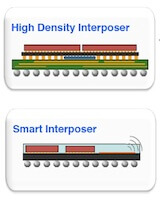
- Cu TSV, AR10
- 2-4-layer routing, thick copper damascene
- Temporary bonding
- Thinning, stress monitoring, warp management
Future work includes smart interposer technology with integrated passive devices, as well as RDL interposers, photonic interposers, and thermal interposers with active heat dissipation.
Leti and 3D Demonstrators
Partitioning, and Wide I/O are Leti’s current pet projects, with a return to via last and what Scannell called ‘monolithic sequential 3D’ also on the 3D Leti Roadmap.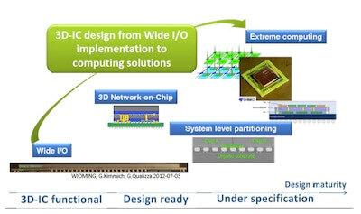
The 3D partitioning demonstrator involves the partitioning of digital on analog, with both top and bottom chips at 65nm. Scannell explained that since analog doesn’t scale well, the idea of this work is that in future nodes, it will only be necessary to scale the digital part, which saves money.

The wide I/O demonstrator — dubbed WIOMING, which stands for Wide IO Memory Interface Next Generation — was developed in cooperation with ST Ericsson, ST Microelectronics, and Cadence Design Systems. It is said to provide a “major breakthrough for energy efficient memory.” Scannell says it looks similar to previous wide I/O demonstrators, but differs in that it is a face-to-back rather than face-to-face configuration.
Next on the Leti drawing board is a return to via last development, this time focusing on making high-density vias that are smaller (3um), using permanent, copper-to-copper bonding via a direct oxide bond that behaves like a solid piece of copper vs. a chain. Demonstrated on 65nm, Leti is reporting good reliability results and according to Scannell, they have “ironed out some of the issues from years ago.”
Leti and Monolithic/Sequential 3D
The best way to explain Leti’s approach to monolithic 3D is through theillustration provided by Scannell.
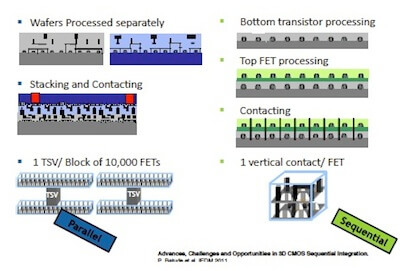 As you can see here, the parallel approach involves processing the wafers seperately, stacking and interconnecting chips, which results in 1 TSV block of 10,000 FETS, VS, A sequential processing approach that results in one vertical contact FET. The first demonstrator of a 3D sequential structure down to LG 50nm has been achieved.
SEMATECH on Metrology
I managed to duck into two of the presentations during SEMATECH’s metrology workshop. From LAM Research, was a novel method for TSV profile metrology using spectral reflectrometry. Here’s what I learned. It’s important to monitor the TSV profile because it has on impact on overall TSV performance. Electrical and reliability performance are dependent on the etch profile control of the TSV, such as the sidewall angle, as well as the thickness of the barrier, seed and isolation layers. LAMS’s solution uses what they call Optical CD concepts, with a modeling approach to calculate the DF spectrum. Future work includes applying a film coverage to the inside of the via, to get a look at systematic defects, and via sidewall roughness.
FEI’s offering to solve the slow pace of metrology is a Plasma Focused Ion Beam (PFIB) technology that brings the site-specific advantages of Ga FIB to package-scale problems. The aim is to enable the kind of structural analysis customers are used to at the packages level. The PFIB system removes materials more than 20x faster than existing FIB technologies, because “more ions in means more atoms out.” In other words, more current equals faster milling. The system can accommodate features from 50-1000um, and allows for trenching through stacked die to reach lower die.
There were many more worthwhile presentations throughout the day. I will be able to provide links to the presentations, available for download, in the next few days. ~ F.v.T.


