


A Solder Bump Expert’s Take on the Expanding World of Advanced Packaging
An interesting take-away from the keynote talk delivered by Brandon Prior, Prismark Partners, at this year’s IMAPS International Device Packaging Conference, held March 11-13 in Fountain Hills, AZ, was the observation that just because new advanced packaging types are being introduced to the market, it doesn’t mean that older ones...

Latest Developments in Cleans for TSVs and Cu Bumps
At IMAPS DPC 2014, which took place March 11-13, 2014, in Fountain Hills, AZ, there were several presentations focused on new developments in cleans for TSVs and Cu bumps for 2.5D and 3D IC processes. Cleans has become increasingly important as bump pitches are reduced and TSVs have higher aspect...

Progress Reports for 3D IC Thermal Management and Test
In Jan Vardaman’s recent readiness report card issued at 3D ASIP in December, 3D IC thermal management issues scored and “F” for lack of a solution o the hot-spot problem when stacking memory on logic. And while she gave 3D IC test a “B” for probe card development, it got an...
What Node Names Really Mean; The TB/DB Saga continues; HMC update
Did you know that when foundries talk about 14nm and 16nm node chips, these devices are in reality no denser than their 20nm predecessors? Or that a particular node name does not reflect the size of any particular chip feature, as it once did? Or that since 2007, the doubling...
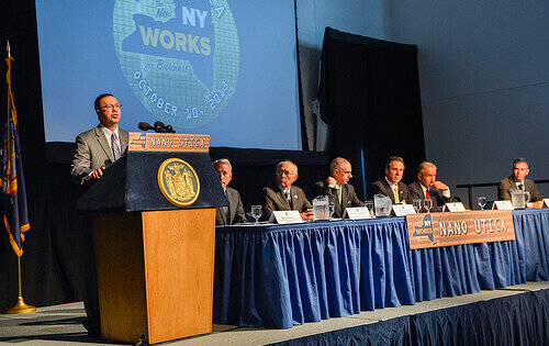
Nano Utica gets $1.5B Infusion; Probably Good Die Revisited; Developments in Monolithic 3D
Word on the street is, New York will soon be known as Nano York, with all the money the state is pouring into nanotechnology research and development. The most recent announcement by Governor Cuomo is a $1.5 Billion Public-Private investment intended to turn the Mohawk Valley (Utica) into the next...
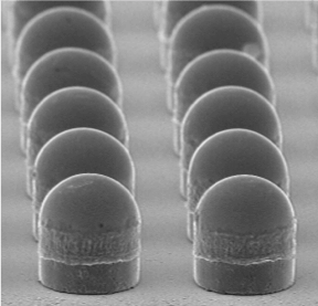
Is it Time for Fluxless Processes for 3D Packaging?
A 3D InCites reader recently inquired whether cost drivers and fine-pitch requirements in 3D applications are moving manufacturers away from flux towards fluxless processes in the bumping steps for both bump formation and assembly.To answer this question, 3D InCites turned to the materials and equipment experts, speaking with Jeff Calvert,...
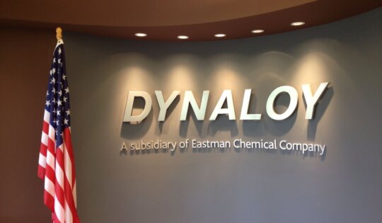
Dynaloy: A Formula for Cleans
It’s hard to believe that inside such a non-descript building set back down a picturesque country lane in (almost) rural Indiana, really cool things are happening. This is the home of Dynaloy, LLC, a subsidiary of Eastman Chemical Company, where innovative chemical formulations are being developed to remove the most...

Understanding The Complexity of Cleans
There is nothing like a little hands-on experience to help someone understand a particular technology better and more fully. Last week I spent two days in Indianapolis learning about how cleaning formulations are made, at the invitation of Steve Dwyer, Business Director Electronic Materials Dynaloy LLC, A subsidiary of Eastman...

SSEC’s New Chemistry for TSV Reveal
This is part of a series of short interviews, based on face-to-face meetings at SEMICON West 2013. SSEC had a lot to celebrate at this year’s SEMICON West, 2013. The company launched two new equipment platforms, WaferStorm and WaferEtch, each configuring single wet wafer processes for specific applications. Two of...
Alchimer Streamlines Wet Approach
Streamlined and versatile: that’s the impression I came away with after talking to Nao Shoda, senior director of business development and technology, Alchimer, about recent developments to further optimize the companies’ electrografting processes for through silicon via (TSV), isolation, barrier, seed and fill steps. I wrote about them frequently in...
Dow Corning offers the Power of Silicone Technology
This is part of a series of short interviews, based on face-to-face meetings at SEMICON West 2013. After my interview with imec’s Ludo Deferm, I met up with Andrew Ho, global industry director, advanced semiconductor materials, for Dow Corning’s Electronic Solutions, to get an update on Dow Corning’s developments in...
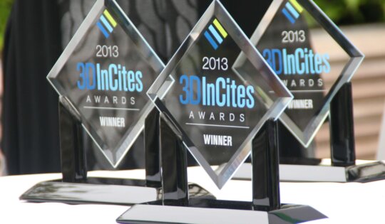
And a Good Time was had by All – 3D InCites Awards Breakfast, 2013
Despite the chilly San Francisco morning temperatures, a sizable crowd of 2.5D and 3D enthusiasts gathered at the Impress Lounge to witness the inaugural 3D InCites Awards Breakfast, held July 11, 2013 during SEMICON West. For me, it was especially significant as it marked four years since I first launched...
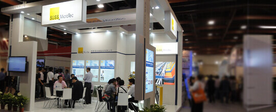
2013 SUSS MicroTec Technology Forum Focuses on 3D TSV infrastructure
SUSS, being an equipment maker addressing various manufacturing challenges faced by 3D IC enablement, definitely has a lot riding on ensuring that all pieces of the 3D IC puzzle are in place. This was evident from the range of presenters they had lined up during this year’s Technology Forum, held...
Momentum Builds for the 2013 3D InCites Awards
Subscribers are practically blowing up 3D InCites as they duke it out online and race the July 3rd deadline for casting their ballots in the public opinion poll for this inaugural 3D InCites Awards; which is great because the first 3D InCites Awards Breakfast, co-presented by 3D InCites and TechSearch...
Dow Corning: Temporary Bonding Solution
Product Description Dow Corning temporary bonding solution is a bi-material silicone based technology featuring low cost of ownership and room temperature bonding and debonding. The chemical and thermally stable materials are spin-on type and can be use for wafer thinning down to 50um providing a global TTV of 2um on...
Triton Micro Technologies: Through-glass-via (TGV) interposer
Product Description Triton Micro Technologies’ ultra-thin through-glass-via (TGV) interposers create 3,000 or more I/O connections per device for high-density IC packaging. Triton uses micro-drilling and via-fill technologies to manufacture 2.5D and 3D TGV interposers for MEMs, RF and optics applications on wafers up to 300mm with thicknesses of 0.7mm and...
Technology Updates at ECTC 2013
The ECTC 2013 stats are in. This year showed increases across the board with: Over 1,300 attendees, the highest attendance ever, from 26 countries 377 technical papers, presented in 36 oral and five interactive presentation sessions, including a student poster session 12 sessions focused on 3D/TSV, including several of the...
ECTC 2013 Interview: Dow Corning throws its Hat in the Temporary Bond/Debond Ring
At ECTC 2013, Dow Corning Corporation (DCC) introduced its solution to the temporary bond/debond conundrum. During the materials and process session, Ranjith John, materials development & integration engineer at Dow Corning, presented a paper titled Low Cost, Room Temperature Debondable Spin on Temporary Bonding Solution: A Key Enabler for 2.5D/3D...
ECTC 2013 Interview: SSEC’s Laura Mauer Talks about TSV Reveal and TSV Clean
This year’s 3D InCites coverage of ECTC 2013 features a series of interviews with suppliers to the 2.5D and 3D IC market. I spoke with a number of exhibiting and attending companies who had progress reports on their tools, processes and materials aimed at leaping over the remaining hurdles. The...

2013 Predictions for 3D ICs as reported by SPN
While most of the semiconductor trade publications wrapped up their 2013 prediction posts by mid January, Semiconductor Packaging News (SPN) forged on with its original annual Viewpoints series right up until last week. I spent some time pouring over the musings of industry executives’ contributions. Many discuss the proliferation of mobile...