
An interesting take-away from the keynote talk delivered by Brandon Prior, Prismark Partners, at this year’s IMAPS International Device Packaging Conference, held March 11-13 in Fountain Hills, AZ, was the observation that just because new advanced packaging types are being introduced to the market, it doesn’t mean that older ones are dropping off or becoming obsolete. As a result, what we’re facing as an industry is an ever-broadening scope of specifications and requirements that need to be accommodated by suppliers. I spoke with Jianwei Dong, Dow Electronic Materials, about this phenomenon in the packaging world, and where it’s headed from the solder bump perspective.
Packaging is not as defined as front-end processes, explained Dong. When it comes to designing materials, every new technology adds complexity; nothing is ever replaced or removed. “Embracing 3D doesn’t mean you give up the previous technology,” he said. “Our challenge is how to maintain an ever-increasing and more complicated portfolio with several integration schemes.”

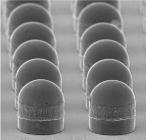
Take the solder bump, for example. For those who don’t know any better, solder bumping appears to be a given. But in reality, Dong explained, every customer has to deal with lots of different geometry, plating nodes and technology nodes. “There’s a whole slew of technology being practiced at the same time,” he said. “We need to make sure our solder chemistry is very versatile as it will be utilized for C4 bumps, but will also be applied to Cu pillar capping, and needs to be ready for micro-bump applications.” One of the greatest challenges is playing to all the different requirements and adjusting the chemistry to different needs (Figure 1).
With regard to the technology roadmap that seems to be transitioning to Cu, and ultimately to Cu-Cu thermocompression bonding, what does that mean for solder? “I strongly believe in the next 3-5 years, solder will still be around because of its unique capabilities,” he noted, citing its forgiving nature that relaxes stress and provides thickness uniformity to bumps.
Dong explained that Dow’s TS 6000 tin-silver chemistry is strong in adapting itself in diverse applications without abandoning existing processes. “This gives our customers the competitive edge.” It is suited to advanced applications of 20-25µm diameter and 50µm pitch. He’s seen it able to handle even smaller pitch sizes and diameters for pillars and capping formed by electroplating. “Our limitation is the test vehicle,” he said. “We can’t get a supplier to provide smaller than a 20µm pillar, but it hasn’t failed yet.”

Dong says he thinks people take solder plating for granted. In reality, if a bumping house or supplier needs to handle a diverse portfolio of products, it can’t design a process just for microbumping applications. There’s always an overlapping technology and need. For example, the focus for microbumps is precision plating, but C4 is about throughput. All this has to be done with a single chemistry, so that’s the process, he said. Once a chemistry is tailored for a specific customer, it doesn’t need further adjustments for specific applications. In this way Dow provides material solutions that provide a lower cost of ownership. ~ F.v.T.


