

At IMAPS DPC 2014, which took place March 11-13, 2014, in Fountain Hills, AZ, there were several presentations focused on new developments in cleans for TSVs and Cu bumps for 2.5D and 3D IC processes. Cleans has become increasingly important as bump pitches are reduced and TSVs have higher aspect ratios. It’s not just about being clean enough, but also about surface preparation for the next process step.
I spoke with John Tracy, of Akrion Systems, to learn more about the company’s cleaning technique that combines megasonics with spray in a single wafer wet process tool to effectively clean thick bump photoresists from microbumps. I first connected with Akrion Systems last fall at IWLPC, where Michael Ioannou, CEO and president of Akrion Systems explained the companies vacuum drying process for wafer surface preparation.
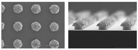
According to Tracy, Akrion “grew up in the front end” developing etching and cleaning processes at the interconnect level. So the company is used to working with fine features. They have recently taken the technology to microbumping, focusing on Cu pillars that are formed using thicker, negative tone or chemically amplified photoresists. As micro-bump pitches become finer, manufacturers are turning to resists that are favorable to cross-linking and maintaining critical dimensions at high thickness, which make them difficult to remove with solvent chemistries alone. Tracy said it can take 20-50x longer to remove negative tone resists.
Akrion’s multi-step process is performed in a four or six chamber single wafer wet processing system. In the first step, the wafer is exposed to solvent reactants by spray-coating the wafer to bring it onto contact with the solvent. Next, a wand transducer that is attached to an RF power supply imparts .85 – 1.0 MHz megasonic energy into the solvent reacting with the photoresist, driving the reaction quickly to the boundary layer at the surface of the wafer. There is no immersion step; solvents are delivered using a spray system. Tracy says the process has been successful on resist masks of 20-50µm thickness, and they have recently tried it on 100µm thickness masks.
“When used in conjunction with a solvent wet chemical process, it helps drive the solvent reaction,” explained Tracy. “The process time is shorter and the chemical consumption is reduced. Shortening process times helps to lower the cost of ownership (of TSVs).”
I asked about the potential of damaging the wafer surface with megasonic energy, and Tracy assured me that while damage when using megasonics can occur at 90nm and below, the dimensions we’re working with in this process are too large to be concerned about damage.
Akrion has been working in partnership with A*STAR-IME in Singapore to develop this technology. Additionally, they recently announced that they’re working with two well-known European research centers to further develop these processes.
Reporting on efficient through silicon via (TSV) resist and residue removal in 3D IC was Dynaloy’s Kim Pollard. Dynaloy has recently been conducting feasibility studies in partnership with SSEC, manufacturer of wet wafer processing systems for semiconductor manufacturing, and in particular, a tool targeting TSV cleans. The paper Pollard presented shows results of ongoing feasibility studies for post-Bosch process residue removal using a solution with an improved environmental health and safety (EHS) profile. I spoke with Kim and Laura Mauer, of SSEC after the presentation to learn more about the work, and future steps.
Pollard explained that in addition to the challenge of effectively removing photoresist residue from high aspect ratio (HAR) TSVs, while leaving the surface in good shape for the next processing steps, additional challenges exist as companies strive to decrease the EHS impact on the chemical formulations being used. DMSO and NMP are a health concern when included in formulated solutions due to their transdermal properties, while TMAH, a commonly used base, is an autonomic nervous system toxin. “They’re great for cleaning, and although they can be handled safely, they’re also great for penetrating the skin,” noted Pollard. “Additionally, NMP has reproductive risks. Dynaloy has developed a new solution that does not contain NMP or TMAH for post-Bosch process cleans. When used in combination with the SSEC tool in a process which involves a soak and high pressure spray, cleaning can be accomplished using an inherently safer proprietary chemistry.”

Another goal of this work, explained Mauer, was to develop a one-step process that removes both the photoresist and the fluorine residue that remains on the via sidewall, post-etch. The current method is a two-step process, in which the photoresist is first removed using an oxygen plasma ash process. Then a wet process is used to remove the fluorine residue. Ultimately, the goal is to eliminate the ash process because it’s expensive, she explained.
Pollard presented two case studies. The first was performed in the Dynaloy lab on wafer coupons that had TSVs with an angular etch structure, and samples showed residual fluorine was present. The residue was successfully removed with the new chemistry.
Case Study 2 was performed at SSEC on their processing tool using full wafers. In pre-clean analysis screens, however, the wafers did not show any residual fluorine was present. When cleaned, there was still no fluorine present. While the second study could not be used to provide conclusive data, the results of the first study was enough to determine that the chemistry works, and that further additional studies in conjunction with SSEC is recommended.
Three questions remain: is the plasma process improved enough so that residue problem is not an issue? Is it a more cost-effective option to use the resist removal process directly and eliminate the plasma step? What effect does surface preparation of the TSV after plasma cleaning or wet cleaning have on an integrated device process?
Mauer and Pollard explained that the next step is to compare different scenarios to determine the effect of cleaning, and which provides the best cleaning results. So they will perform the studies using ash and wet clean processes; wet clean only processes, and ash only. If the cleaning and surface preparation effect is equal, then they will do cost modeling to determine which provides the best cost of ownership. The bottom line, Pollard noted, is that the chemistry appears to work as good as if not better than TMAH based chemistry, which is good news for meeting EHS requirements. Stay tuned as the story unfolds. ~ F.v.T.


