The Microelectronics Packaging and Test Engineering Council (MEPTEC) held its annual heterogeneous integration symposium at SEMI’s headquarters in Milpitas, CA on December 5, 2018. Many manufacturing and test, as well as electronic design automation (EDA) and IC design experts, got together to present and discuss how to integrate heterogeneous functions in advanced IC packages to better meet customers’ expectations for shorter lead times, lower cost and higher performance per Watt of complex system-level solutions.
Market Drivers
The speakers in Session 1, chaired by Dan Tracy, outlined current market drivers and why closer cooperation across the entire supply chain is needed.
Keynoter Risto Puhakka, VLSI Research, confirmed that the semiconductor industry is still booming, but warned that geopolitical turbulence, trade tensions, and significant tariff increases may trigger an industry slowdown. He highlighted the importance of new technologies to better serve applications like artificial intelligence (AI), 5G phones and electric vehicles. These will drive revenues and new requirements for cost-effective integration of heterogeneous functions in ICs.
Figure 1 shows how advanced IC package types, using area array footprint and through silicon (TSV)-like interconnects (flip chip, fan-in and fan-out-wafer-level packages (FOWLP)) are likely to reach a market share of 40% by 2022.
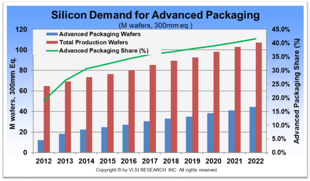
Puhakka also showed that memory sales have been declining in 2018 much more rapidly than other functions. Due to declining memory prices, semiconductor revenues from $B 486 in 2018 will dip to 481 in 2019 and rebound to $B 513 in 2020.
Dongkai Shangguan, VP at Flex, outlined the broad range of Flex’ capabilities, then pointed out that heterogeneous integration isn’t new for our industry. System-in-package (SiP) solutions have been serving a wide range of applications for many years. However, increasing signaling speeds and power supply integrity challenges, as well as cost, space, temperature and schedule constraint, s demand more advanced IC packages.
Jan Vardaman, TechSearch International Inc., explained that economics is the key driver for heterogeneous integration in advanced IC packages and explained how AMD, Google, Intel, Nokia, Nvidia, Xilinx, and others have used silicon interposers (l/s <1mm) or organic interposers (now approaching l/s of 2mm) to design high-performance solutions. She also showed how fast wafer and panel-level packaging are winning market share.
The Importance of Planning And Design Tools
Session 2, organized by me, focused on conveying how important planning and design tools/methodologies are for design and test of ICs, advanced packages and chiplets (bare die, thoroughly tested building blocks for multi-die ICs).
In his keynote, Keith Felton presented how Mentor, A Siemens Business, supports the integration of heterogeneous functions in advanced IC packages. Compared to traditional ways of IC and package design as well as current practice in manufacturing and test, the new methodologies represent big disruptions. Package planning and design steps are becoming much more complex and more like die design steps. User-friendly die – package – board design flows enable developers to optimize the entire single or multi-die IC design by trading off constraints between die, package, and board, to reach performance and cost targets faster.
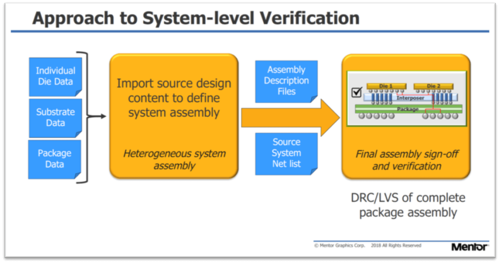
Just like process design kits (PDKs) are enabling accurate, reliable and cost-effective silicon designs, now assembly design kits (ADKs) from leading OSATs provide accurate and current data about materials characteristics and manufacturing/test capabilities. This approach minimizes iterations between design and manufacturing experts and leads to a lower unit cost. It also enables meaningful system-level verification and avoids problems with single and multi-die ICs when deployed in the actual application (Figure 2).
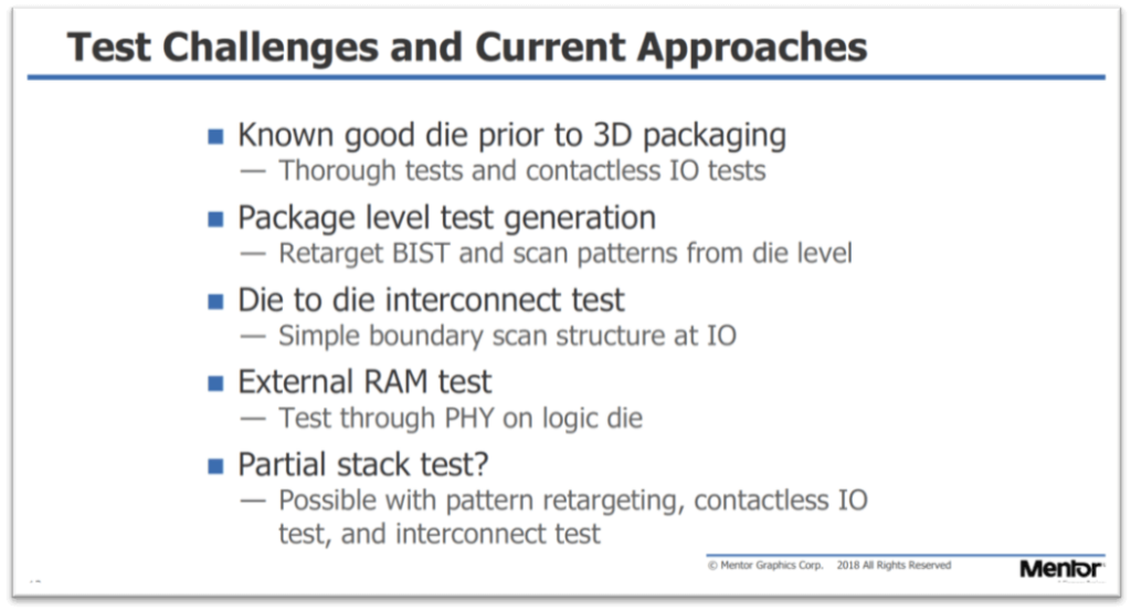
Felton also addressed key points to consider for testing ICs in advanced packages (Figure 3).
Last, but not least, Felton explained how Mentor’s OSAT Alliance Program broadens and intensifies their cooperation with OSATs, accelerates package design projects and brings wafer-level packaging technologies to market faster.
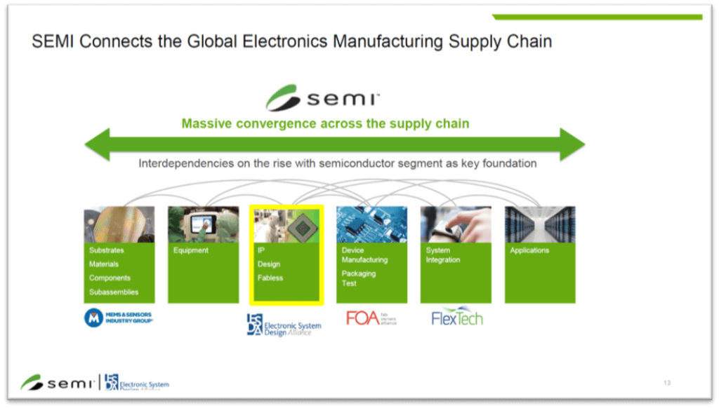
In Spring 2018 SEMI and the Electronic System Design Alliance (a.k.a. EDAC) announced a strategic partnership to bring design and manufacturing experts closer together. Bettina Weiss from SEMI and Bob Smith from the ESD Alliance presented why and how this partnership benefits the members of both industry organizations. Figure 4 shows how SEMI’s reach now spans all relevant design, manufacturing and deployment steps in the semiconductor supply chain.
This strategic partnership and the to-be-agreed-upon technical hand-off criteria, as well as business models for closer cooperation between companies across the entire semiconductor supply chain, are likely to replicate today’s highly successful cooperation between fabless IC vendors and wafer foundries for die – package – board – system solutions.
John Park and Lisa Jensen presented how Cadence supports heterogeneous integration in advanced packages. Park showed the audience how he experienced our industry’s changes and projected next steps (Figure 5).
![[err-ad-fallback-title]](http://www.3dincites.com/wp-content/plugins/a3-lazy-load/assets/images/lazy_placeholder.gif)
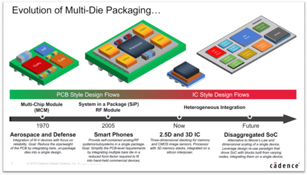
Park mentioned that multi-die IC design capabilities have reached very impressive levels, e.g. completing 800M connections in a recent design. Design planning and optimizing at the start of a project now takes up to 60% of package designers’ efforts. Also, sign-off quality verification of the entire design plays a more significant role. It avoids costly re-spins and schedule slips. Park pointed out that Cadence sees many designs that require analog and RF functions to be added to the digital cores of a multi-die ICs and outlined tools and flows Cadence offers to integrate heterogeneous designs up to very high complexity.
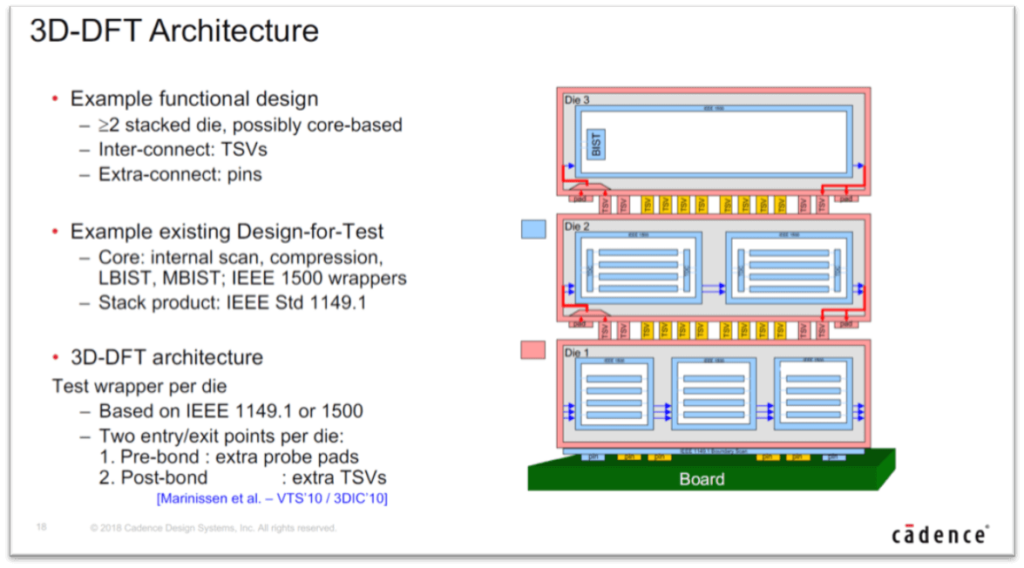
Lisa Jensen is well-known among IC test experts. She presented Cadence’ design for testability concepts and explained their benefits. Figure 6 shows how a “test elevator” is applied to thoroughly test all die in a 3D-IC. Jensen demonstrated her expertise in design for test, vector generation and debug methodologies.
Advancements in Assembly
Session 3, chaired by Joel Camarda, focused on important advancements key assembly equipment vendors achieved.
Horst Clauberg, Kulicke & Soffa, stated that wire-bonding is still the dominant methodology, but thermal compression bonding and especially Xperi’s direct bond interconnect (DBI™) are rapidly gaining market share. Clauberg emphasized that K&S introduced laser assist processes to improve bonding and die-placement accuracy.
Chris Scanlan, SVP at Deca Technologies, explained Deca’s Adaptive PatterningTM technology and how it increases die-placement accuracy and with it, manufacturing yields.
Supply Chain Challenges
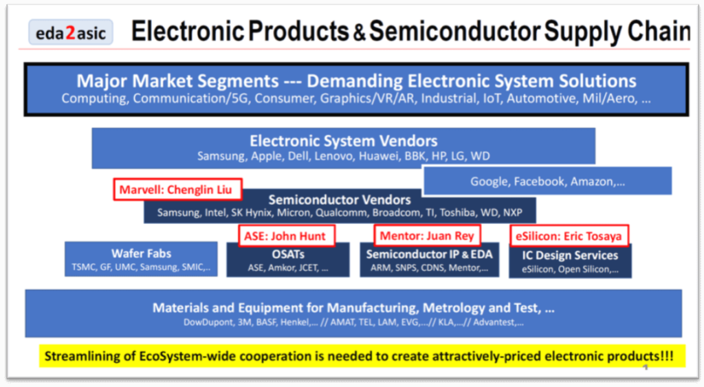
Session 4 was a panel discussion, centered around supply chain challenges for advanced packaging. Ed Sperling, Editor in Chief of Semiconductor Engineering, was the moderator. Figure 7 shows the panelists, their affiliations and how all the semiconductor supply chain pieces they represented, fit into the electronic product’s ecosystem.
Sperling asked the panelists to comment on market trends, their current experience with traditional and new design methodologies, to compare capabilities of different package types and their views about chiplets (a.k.a. “LEGO-blocks” for multi-die ICs). In response to Sperling’s and audience questions, a very informative discussion developed. It clearly showed that all of the panelists are true experts in their fields and the previous sessions raised the audience’s interest in advanced packaging and heterogeneous integration.
However, in my view, this panel discussion also confirmed that a lot of work still needs to be done before the existing suppliers and customers can cooperate effectively and efficiently. After fine-tuning the ecosystem for decades to crank out billions of smartphone chips, now we need to adapt to changing market demands for much lower volume designs and much more diverse applications. A better understanding of system-level challenges and closer cooperation between planning/design and manufacturing/test experts is needed to serve the new requirements better.
Based on my 25+ years of experience with refining ASIC technology and business models, as well as many years of working on the fabless and foundry cooperation, I am optimistic that our industry will master the current supply chain challenges with single and multi-die ICs, utilizing advanced packages, as well. A very big step to accelerating these changes is the expansion of SEMI’s traditional manufacturing focus to include EDA and IC design. Among other strengths, SEMI is well known for encouraging cooperation and developing industry standards. Both are key elements for the success of this transition.
See the press release about SEMI winning the Electronic System Design Alliance as a Strategic Association Partner here and my recent blog about this very synergistic partnership here.
Thanks for your support and all the best for 2019. ~ Herb