
MEPTEC lunches, now known as the MEPTEC / IMAPS / SEMI Semiconductor Speaker Series Luncheon sponsored by Chip Scale Review, are on again in Silicon Valley. At the most recent lunch in mid-March 2018, I was pleased to see that it was none other than Rich Rice, VP Business Development, ASE US, delivering his view on Packaging Innovation for our Application-Driven World
Rich’s thesis: that, despite excellent aggregate market performance for semiconductors in 2017 as a result of electronic market dynamics (positive) and overall economic buoyancy (improved), we may see challenges in 2018 because some of the largest semiconductor revenue drivers, smartphones notably, are flattening.
What’s an industry to do? According to Rich, we must collectively identify and nurture new applications that can stimulate further growth, and we must collaborate across the supply chain to drive and sustain the new advanced semiconductor / advanced packaging-based solutions at the base.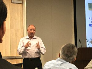
We’ll be applying less emphasis on classic Moore’s Law progress and rather more emphasis on system-level integration technologies, with the outsourced semiconductor assembly and test service providers (OSATs) and electronic manufacturing service (EMS) houses pushing values up and costs down by implementing new integration and miniaturization technologies for system-in-package (SiP) and for system-in-module (SiM).
We’ll achieve the next level of system performance through package-level homogeneous, and package-level heterogeneous, integration.
And that’s music to 3D InCites’ ears.
There is, said Rich, “Tremendous momentum behind fan-out today,” fan-out delivering, along with some of the other advanced packaging technologies, notably 2.5D (henceforth to be known as enhanced 2D) and 3D integration, a simultaneously optimized solution for higher performance – increased bandwidth – lower latency – reduced power consumption and mixed process node / mixed functionality in your next packaged microelectronic product.
Is there one packaging technology to rule them all, one packaging technology to bind them?
Rich thought not; for any given packaging application, it will be the packaging technology bringing the needed level of performance at the best price that will win.
Which is why Rich reminded us to not forget about wire bonding! “At ASE we’re still investing in wire bonding capacity.”
Wire bonding: it’s mature, it’s reliable, it’s easy to use, it’s low cost, and there is a HUGE installed wire bonding capacity.

It’s just that I’m old school like that.
MEMS devices and optical sensors are of ever-larger importance to our world and thus comprise an ever-growing portion of ASE’s business, something that has resulted in ASE developing new die-package interaction simulation and design tools, new packaging materials, new molding technologies, including film-assist molding for creating the specialized ports needed by MEMS microphones and pressure sensors, and new dicing techniques.
And for some of the RF applications of importance, including upcoming 5G applications, there’s new thinking about EMI shielding, and about integrated antennas.
Regarding collaboration, Rich’s three examples included the new TDK – ASEEE (ASE Embedded Electronics) joint venture for embedded packaging solutions that just went live in Kaohsiung Taiwan; ASE’s work with Deca Technology and Deca’s adaptive patterning IP (“A game changer” for cost-down panel level packaging), a packaging technology going into production imminently with a key lead customer; and ASE’s work with Cadence Design for next-generation SiP design tools.
Rich sent a special shout-out to 3D InCites’ own Herb Reiter for pushing (and pushing) the packaging and design tool industries toward this important collaboration. Well done, Herb!
In conclusion, Rich offered these takeaways: expect semi growth to moderate in 2018; end application needs continue to drive very different packaging technologies (which is why there are still many different packaging technologies); we must continue to advance existing semiconductor device packaging platforms and leverage them for our benefit; we must collaborate for success.
From Santa Clara, CA, thanks for reading. ~PFW


