


As it has for the past 14 years, the global microelectronics industry gathered at Wekopa Resort and Conference Center in Fountain Hills, AZ, March 6-8, 2018, for the 2018 IMAPS Device Packaging Conference (DPC) to share knowledge, discuss strategies for growth, learn about the latest heterogeneous integration from fan-out wafer level packaging (FOWLP) to 3D ICs. We also managed to get in some golf and hiking on the side (or as we like to call it “networking time.”)
With the impending publication of the newly inked heterogeneous integration roadmap (HIR), scheduled for release in May 2018, the agenda for the 2018 IMAPS Device Packaging Conference was deliberately designed to inspire pause and reflection. From the keynotes to the panel, we were challenged to remember how we got here, what is working, what’s not, and what’s next.
The Vertical Journey
Phil Garrou opened the event with a refresher course on 3D IC. We’ve been spending so much time over the past few years talking about fan-out wafer level packaging (FOWLP), it was kind of fun to reflect on the good old days, back when we made predictions that didn’t exactly unfold as planned. Even so, for me, it’s pretty cool to see how far 3D has come, and to have been part of this journey for the past nine years.
We jumped in the WABAC Machine with Phil, traveling from 1980 (way before MY time in this industry…) to now, exploring our quest for miniaturization, first by shrinking the whole package, and then by going vertical. (In Japan, Phil noted, they called it “downsizing” until someone explained the negative implications of that). In 2005, Phil predicted the vertical trend would evolve in three ways; wire bonding, package-on-package (PoP), and 3D ICs using through silicon vias (TSVs).
Phil reminisced about the early pioneering work of Mitsumasa Koyanagi, Tohoku University; and Peter Ramm at Fraunhofer IFT and Siemens in the 80’s and 90’s, and a 2001 IEEE paper written by researchers at Stanford, MIT, and Georgia Tech about interconnect limits on gigascale integration in the 21st century. It predicted that on-chip interconnect would decelerate, and 3D IC should be explored to alleviate interconnect delay and density problems. Those were the good old days when everyone was fired up with the possibilities.
Then reality hit. Remember in 2006 when Samsung’s CEO said the company was ready to go with 3D ICs? Yeah, me too. Didn’t happen, as Phil noted. The company was going to put TSVs in NAND flash memory, but it cost too much to build for a low-cost technology. Or when 2007, Intel announced it had developed 3D IC on 300mm wafers in 2007? It was rumored that it would show up in Ivy Bridge in 2012, (it didn’t) and in Haswell in 2013 (it didn’t). Phil also reminded us about WIOMING, which “appeared on 2013, and then disappeared again,” he said. And what the heck happened with Micron’s hybrid memory cube (HMC)? According to Phil, it no longer exists and Micron is working on a next-generation version of some kind.
Yep. 2012-2014 were disappointing years, noted Phil. Except that during that time, the kinks were worked out of enabling technologies like via etch, wafer thinning, temporary and permanent bonding, and processes of record were established.
The big 3D TSV breakthrough came in high bandwidth memory (HBM) in 2014, and then the real products began rolling in 2015: Sony’s CMOS image sensors that stacked pixels on a separate layer from the circuitry; graphics modules from NVidia and AMD that integrated HBM stacks on an interposer with the GPU; and stacked memory for high performance computing (HPC) in Intel’s Knight’s Landing and Zenon Phi.
That said, we are still dealing with supply chain complexities, noted Phil. Si interposers availability is limited to TSMC, Globalfoundries, and UMC. And as Mark Bohr noted back in 2012, unless we see cost-cutting measures, 3D ICs may remain relegated to high-end applications.
Some say they came away from Phil’s keynote feeling like 3D hasn’t happened at all – I disagree. It just didn’t happen as fast as we expected or how we predicted. Is success only measured in high volumes of low-end devices? Not necessarily. As HPC volumes increase driven by artificial intelligence, bitcoin, autonomous vehicles, and other data-hungry applications, then the volumes of 3D ICS will go up, unless, of course, there is another way…
Advanced Packaging Alphabet Soup Revisited
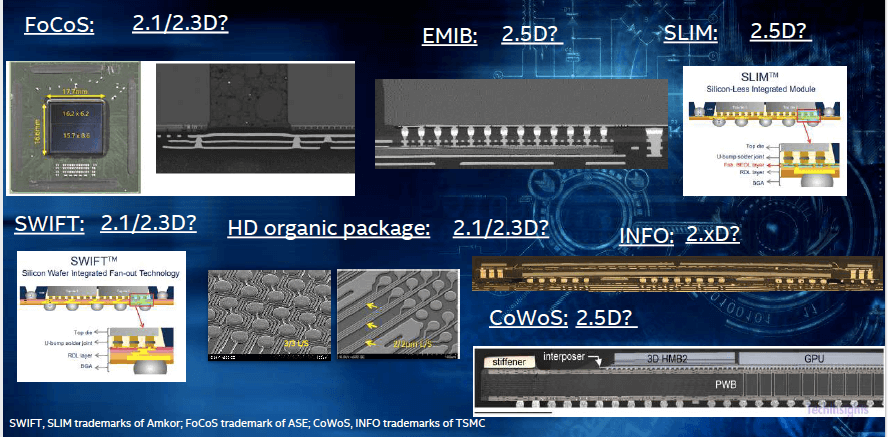
Phil’s keynote set the stage nicely for the next speaker, Intel’s Raja Swaminathan, who talked about the Age of Data that is calling for greater computing power and improved memory performance. All this, he said, points to heterogeneous integration as the solution. His rising stars include a host of organic and silicon substrate-based architectures including Infineon’s eWLB, ASE’s FoCoS, Amkor’s SWIFT and SLIM, Intel’s EMIB, TSMCs InFO and CoWoS, and Deca Technologies M-Series (not shown).

Like Phil, Raja scoffs at term, ‘2.5D’. “2.5D is not based in physics. It was coined as a joke!” he said, citing, like Phil, the time in 2009 at the 3D ASIP conference when Ho Ming Tong, ASE, first used the term. (Ironically, at that conference, Tong also predicted the end of scaling to be 10 years away and 3D to be ubiquitous.) Raja also says we should get away from the interposer nomenclature. “It’s either active or passive silicon,” he said.
Those dimensional jokes have continued and confused many, so the IEEE and SEMI have assembled a working group to spearhead HIR and create a whole new nomenclature that does away with fractional dimensions. Heretofore, the industry will refer to 2D, 2D enhanced (formerly 2.5D) and 3D architectures. 2D enhanced will be further categorized as 2DS (silicon substrate) or 2DO (organic substrate).
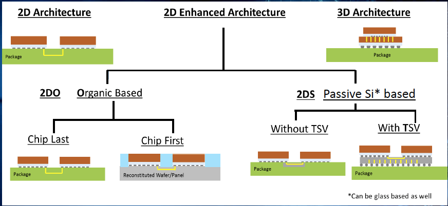
Probably one of the most beneficial and educational discussions I had at DPC was with Raja, who sat down with me to define the main difference between 2D and 3D architectures once and for all. It really is quite simple: when active dies are placed side-by-side and connected through the package, whether it’s on an organic or silicon substrate, its 2D and 2D enhanced. “When two or more active pieces of silicon talk directly to each other without a redistribution layer (RDL) that’s 3D,” said Raja. “Mechanical stacking is one thing – but if you’re not connecting in 3D It’s not a 3D architecture.” In other words, by these new definitions, package on package (PoP) is not officially a 3D architecture.
Moreover, higher linear densities will differentiate 2D from 2D enhanced, explained Raja. Linear density refers to the number of wires escaping per millimeter of die edge and is the key metric used to compare 2D architectures. It is not an applicable metric for 3D architectures, he added. Areal density, aka bump pitch, is a differentiator for 3D.
While I’m all for putting to rest the term “2.5D interposer”, I’m not completely sure that the way to solve the advanced packaging alphabet soup situation is by adding MORE acronyms to the nomenclature. But hey, I’ve been wrong before! One thing is for sure, it will require an enormous effort to educate the industry. You can be sure we’ll be talking about it much more on 3D InCites. After all, that’s what we are here for!
And that was just the first day! There’s plenty more to come from the panel, sessions and general business council. ~ FvT
PS: The feature photo was snapped in the Wekopa Conference Center parking lot by Martijn Pierik, Kiterocket. Will the owner of the car step forward? You’ll be featured in next year’s 3D InCites Awards Quiz.


