
Day Two of the European 3D TSV Summit dawned bright and clear, with such a spectacular view of the nearby French Alps that it took real commitment to stay indoors and focus on the task at hand. But I have to admit that for the most part, it was worth the sacrifice to hear what this collection of speakers had to say.

Georg Kimmich, head of Silicon Packaging R&D at ST-Ericsson delivered a dose of harsh reality in his keynote address, when he explained why wide I/O – long thought to be the killer app that would catapult 3D ICs into commercialization inside smartphones – hasn’t happened yet. ST-Ericsson was part of the very successful WIOMING project that was a collaborative effort with Cadence, ST Microelectronics, and CEA Leti (Figure 1).
According to Kimmich, the hold-up has been due to a number of things including a complex business model, the availability of LPPDDR3 and 4, which offer comparable bandwidth at a lower cost, and thermal performance issues.
Offering the end-customer perspective, he explained that while the consignment model is considered as a sole solution to be acceptable by all three parties involved, the end-customer has to push and pay for it. The memory supplier has to be okay with late payment after assembly and test, and yield compensation issues need to be worked out.
And as great as Wide I/O is, he questions whether we will really need all the bandwidth future projections suggest. Rather, ST Ericsson’s approach is currently to build more efficiency into the system, thereby reducing memory bandwidth requirements and make a cheaper solution.
So was Wide I/O a bad dream? Not at all, says Kimmich. While in his estimation it will be two or 3 years before we see it in smartphones, there are many products that will benefit from derived technologies very soon. The company is working on a 3D Logic on AMS prototype, leveraging 3DTSV and backside processes, which he says are ready for mass production.
Brandon Wang, of Cadence, echoed some of Kimmich’s sentiments as he presented how EDA solutions can help relieve some of the challenges. “3DIC is a bridge for “More than Moore” solutions, and will provide cost advantages in the long run.” He said, adding that the WIOMING project was a good experiment for testing out 3D technology on the application side.
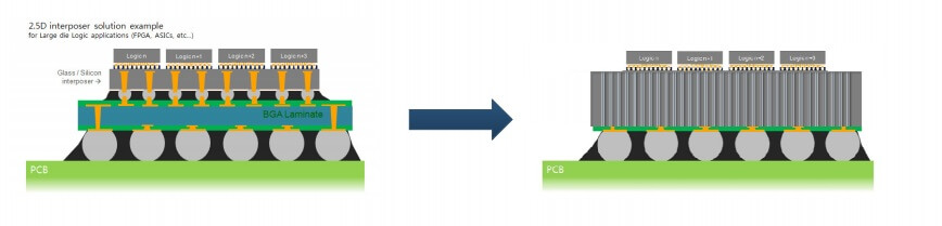
The presentation by Thorbjörn Ebefors of Silex Microsystems, was a great reminder that #1: this symposium is titled the European 3D TSV Summit – not the 3D IC summit, and that #2: there are other market applications where TSVs are already a viable manufacturing solution – MEMS being one of them. Eberfors talked about the “other” markets where TSVs are making a splash including MEMS, LED interposers, for MEMS-ASIC interposers, as a high-density alternative to TMV for PoP or fan-out wafer level packages, or FOWLP, and finally as “the next frontier” TSVs directly into CMOS. Depending on the technology, noted Eberfors, either TSV first or TSV last is implemented.
Silex has been particularly active in developing rigid interposer technology, to create an all-silicon package (Figure 2). Eberfors talked about how integrating functionality into the interposer, new categories of heterogeneous devices can be manufactured. (This concept aligns with Leti’s vision and description of what they call an “active interposer” that I wrote about here, in my coverage of Nicolas Sillon’s keynote address at IWLCP 2012.)
ST Microelectronics’ Jean Michailos created quite a stir among attendees after announcing that the company has recently demonstrated high-yield 3D TSV processes on 28nm FD-SOI. ST Micro has invested aggressively over the years, being some of the earliest adopters of TSVs for CMOS image sensors.
Michailos noted that currently, the driving applications at STM Micro for 3D integration include analog and digital partitioning and Memory on an application processor. Further development is being done to realize such opportunities as passive and active interposers; photonic/electronic partitioning where TSVs are implemented in a photonics die; and 3D network on a chip where 3D is part of the power distribution.
Speaking specifically on the topic of collaboration in the European 3D market, John Greenwood of GlobalFoundries reiterated the company’s devotion to an open collaboration model, saying that value is created when working in a shared risk/reward environment.
Greenwood touched on a number of European projects to illustrate this open model. He identified both Fraunhofer IZM-ASSID and imec as “core partners”, and talked about recent engagements, such as a project with Fraunhofer IZM-ASSID on TSV integration into a 28nm high-k metal gate (HKMG) device wafer to enable 3D chip stacking. With imec, they collaborated with Amkor to develop a 2.5D interposer test vehicle.

Flexibility is a key element, noted Greenwood, explaining that at GlobalFoundries, it’s the customer who decides the engagement level and supply chain of choice. “When the customers collaborate closely, the level of engagement is so much deeper,” he noted. “An open supply chain is exciting to the customer.”
The last few presentations of Day Two were dedicated to updates in the reliability, test and inspection areas, and the progress made in these areas is encouraging.
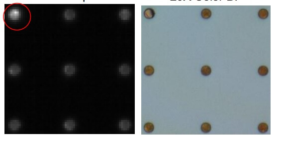
Rajiv Roy, of Rudolph Technologies, talked about the company’s in situ inspection metrology and software solution for TSVs and lithography for under bump metallization (UBM) and RDL metal thickness. With HVM looming close, one of the key challenges is to augment high-speed inspection during HVM such that throughput is 25-30 wafers per hour.
One area of expertise for Rudolph is in inspection of nail protrusion after the via reveal step. Bad vias are detected using a darkfield inspection technique, explained Roy and defect images can be captured in brightfield color. (Figure 3) Other areas of focus for Rudolph include debond inspection, edge-trim metrology, chip-o-wafer alignment, and encapsulation inspection. (Also presenting in the area of TSV inspection was Gilles Fresquet of Fogale Nanotech. You can read my interview with him here.
The test guys are starting to get a complex, because not only is test the last thing to be considered whenever there are new technologies developed in semiconductor manufacturing, its also the last topic to be addressed during a conference. So the last three presenters were not only charged with providing compelling and new information, they had to deliver it in a manner that would keep the remaining attendees alert and interested. Eric Jan Marinissen of imec; Gary Fleeman of Advantest, and Jim Quinn of Multitest did just that. (Although Quinn gets the award for the most animated presentation by using Prezi rather than Powerpoint to create his slides. Aside from causing a little motion sickness from watching the slide changes, he did keep us all alert.)
Marinissen’s presentation discussed how logic-on-logic stacks allow us to define design for test (DfT) by identifying potential test moments and the challenges associated with them. For example, the pre-bond test challenge is microbump probing on the non-bottom die. Testing mid bond requires coordination of DfT up and down the stack. He explained how TSVs are used as test elevators (although unlike real elevators, they don’t use the same TSV for both directions, but rather one for going up and one for coming down. He joked that perhaps he should have called them “test escalators?”) And final test involves testing not just the die, but the interconnects as well.
Reporting on the status of EDA for DfT, Marinissen said a DfT Architecture developed in collaboration with imec and Cadence was released in 2011. It has been extended to include DfT insertion for Wide I/O interconnect test, Wide – I/O interconnect ATPG and test migration, and automated DfT insertion for embedded IP cores, TDC and multi-towers. This DfT Architecture has been implemented in both TSMC’s reference flow 12 and its CoWoS reference flow.

Gary Fleeman and Jim Quinn each addressed the topic of Known Good Die (KGD) and Known Good Stacks (KGS) from the perspective of the equipment suppliers. Fleeman said that when testing a multi-die product, you must consider the accumulated yield. Even assuming you have a perfect interposer, a 5-die stack could have a 4-5% final yield loss. While there are workarounds that allow for continued use of a conventional test flow, they may come at a yield penalty that takes KGD from “probably good die” to ‘maybe good die.” Fleeman says KGD is essential to making 2.5D and 3D cost effective, and therefore requires a “non-conventional test methodology that enables KGD.” “Each interim product must be a known good product.” Fleeman referenced the new test points identified by Marinissen and said that these will be selectively implemented. Each flow will use different points; no flow will use all points.
Quinn echoed Fleeman’s point that we need to think about a known good stack. He recommended leveraging high volume manufacturing practices developed for MEMS manufacturing. There are lessons to be learned there such as dealing with tri-temperature applications, a need for sophisticated backside support for bare die, high compliance probes to accommodate for deflection that contact with low force but ensure best yield.
And that pretty much wraps up my event coverage for the European 3D TSV Summit. Until next year! ~ F.v.T.


Nice report Francoise! Thanks for doing this for those of us who can not be there. The test issue and the business model / ownership issues are not going to be easily resolved.