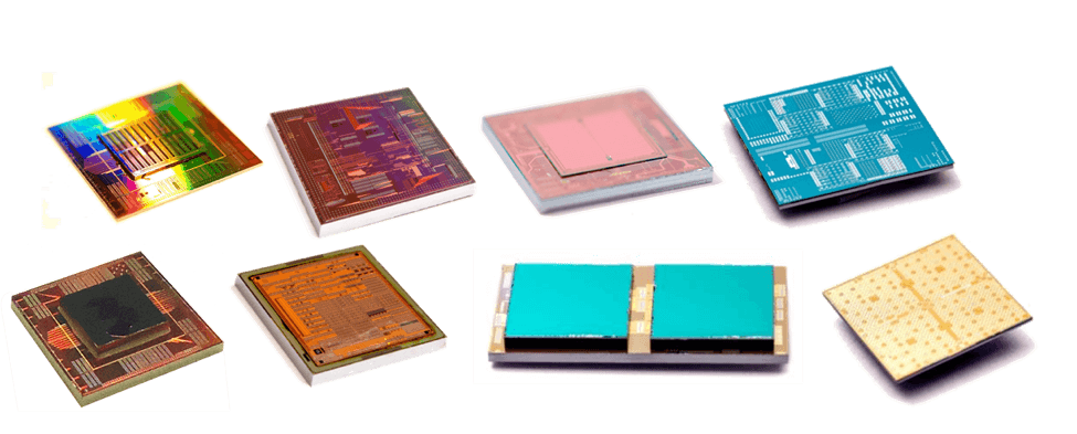
Stacking chips on top of each other (aka 3D stacking) is a well-known approach to make more compact and powerful systems. Until now, it was impossible to probe the large arrays of fine-pitch micro-bumps on advanced chips before stacking. This had a negative effect on the compound yield (because of including faulty dies in the stack). Imec, together with FormFactor (formerly Cascade Microtech), has developed a unique fully-automatic system to probe these micro-bump arrays.
The challenge
Stacking chips in 3D packages is seen as the way forward to building more powerful systems. It compensates for the laws of physics that threaten to push chip makers off the path of Moore’s Law. You could say that 3D unites different technologies and in this way is an important enabler for future Internet of Things products where miniaturized systems based on different technologies will make their mark.
.As an emerging technology, 3D stacking still has many open options and technical challenges. One of these is the probing of chips before being stacked, to be able to test chips for manufacturing defects, and hence ensuring a good yield of the 3D chip stacks. The inter-chip connections are made by large arrays of fine-pitch micro-bumps and it was considered ‘impossible’ to probe these bumps because they are so numerous (≥ 1000) and so close to each other (≤40 micrometer). The current solution is to add dedicated probe pads to the chips, but this requires extra space and design effort and leaves the micro-bumps untested.
The solution
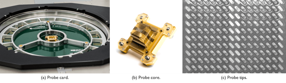
In 2010, Cascade Microtech (now FormFactor) and imec started their collaboration to tackle the fine-pitch micro-bump probing issue. FormFactor provided prototypes of their advanced Pyramid Probe® Rocking Beam Interposer (RBI) probe card technology. This probe card technology contains an IC-design-specific probe core which includes a thin film with MEMS-type probe tips. The high-density probe cores support >1,200 core I/Os. The RBI probe tips require less than 1 gf/tip to make proper electrical contact. The heel of the tip makes physical contact with the wafer, such that the probe mark is typically only 6 × 1 micrometer.
To prove the feasibility of micro-bump probing with these probe cards, a unique full-automatic test system was built consisting of (1) a dual Cascade CM300 probe station from FormFactor (Germany), (2) a hard-docking STS test head with PXI test instruments from National Instruments (Texas, USA), (3) a test head manipulator and docking interface from Reid-Ashman (Arizona, USA), and (4) test program and data analysis software based on LabVIEW and developed at imec (Figure 1).
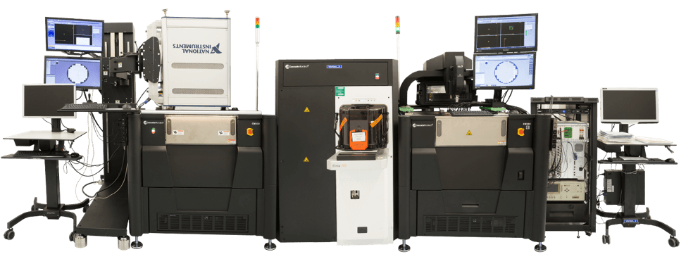
The Cascade CM300 probe station from FormFactor is the basis of our test system (Figure 3). Installed in the clean-room of Fab-2 of imec in Leuven is a CM300 in dual prober configuration. It consists of two probers around a central material handling unit (MHU), a.k.a. ‘auto-loader’. The two probe stations are mostly identical. Both accept ø200mm and ø300mm wafers from the shared MHU, but also have their own front-port for manual loading of ø200/ø300mm wafers as well as SEMI G74-0669-compliant tape frames for (thinned) wafers up to ø300mm. Both probers support four cameras: (1) a top-view camera on the bridge, (2) a platen camera, (3) a chuck camera, and (4) a side-view camera (‘ProbeHorizon’). Both systems handle vertical, non-see-through probe cards through software overlay of images from the platen and chuck cameras (‘MicroAlign’), and both feature an anti-vibration table, a thermally-controlled wafer chuck (-60. . .+200 °C), and a GPIB command interface.
The left-hand prober is adapted for large-array fine-pitch micro-bump probing. It has a 1,224-channel test system connected to it. Due to their large number, cable connections between test instrumentation and probe card would be impractical here and hence have been replaced by the pogo pins of a hard-docking test head. To make space for the hard-docking test head, the left-hand prober does not have the default microscope bridge and top-view camera; the platen camera is the only remaining downward looking camera.

The NI STS test head is a T2 model that contains two PXI racks with test instruments. Rack 1 holds instruments for parametric and functional tests. Rack 2 is dedicated to micro-bump probing. It contains a PXI-4072 digital multimeter (DMM) connected to an ultra-wide switch matrix consisting of nine concatenated PXIe-2535 modules (SMX1–9) of 136 output columns each. This allows them to connect to each of the four channels of the DMM under software control to any of the 9×136=1,224 SMX output columns. The system supports two-point and four-point (Kelvin) resistance measurements between any pair of probe tips (for daisy chains) as well as between a single probe tip and all other probe tips ganged (for characterization of that single probe tip when all probe tips are shorted through the probed wafer).
The experiments
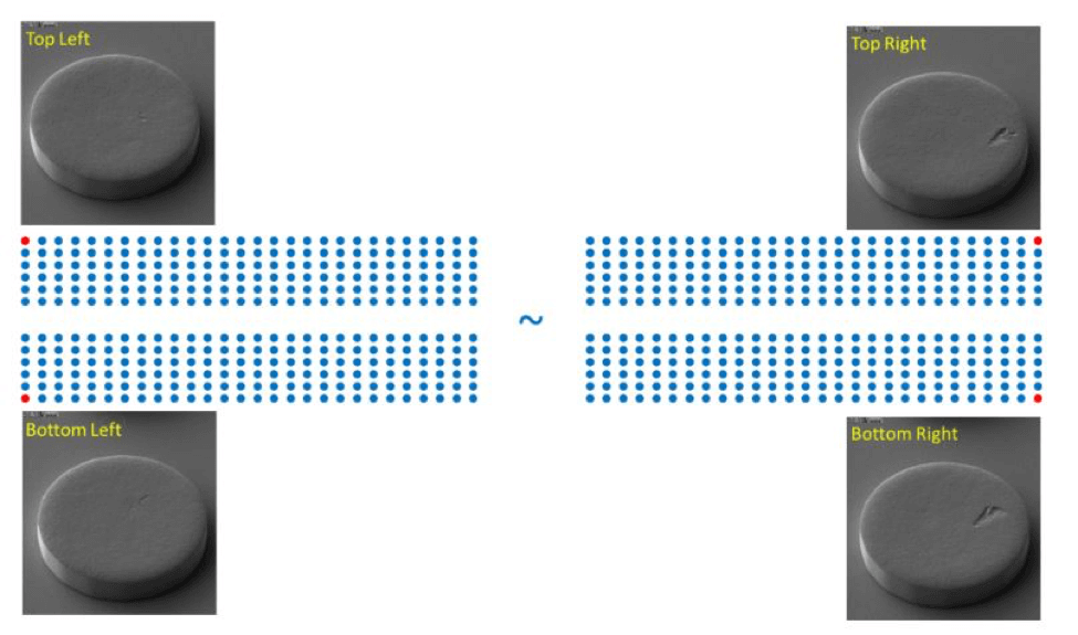
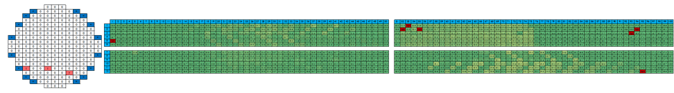
The test system was installed in imec’s clean room to perform experiments. It was successfully used for micro-bump arrays as defined by the JEDEC standardization organization for Wide-I/O single data rate DRAM memories. Both JEDEC’s WIO1 and WIO2 micro-bump arrays were successfully probed, with a minimum pitch of 40µm and a maximum array size of 1200 (= WIO1) and 1752 (= WIO2). ‘Successful’ in this context means that the test system has a sufficient number of channels for the number of micro-bumps; all the probe tips land on the micro-bumps and make good electrical contact, without damaging the micro-bumps; and – last but not least – the approach is economically feasible.
All tests were performed on 300mm test wafers, designed and manufactured at imec and containing micro-bumps with various metallurgies, pitches, diameters, and array sizes (figure 5). The system is now being used routinely to test imec’s micro-bumped wafers. While today’s advanced micro-bump processes are at 40µm pitch, this is, as everything in the semiconductor world, subject to miniaturization. Hence, imec and FormFactor have already started to probe micro-bump arrays at 20µm pitch.
Acknowledgments
This work was done by Ferenc Fodor, Bart De Wachter, Erik Jan Marinissen (imec), Jörg Kiesewetter (Cascade Microtech GmbH), Eric Hill, and Ken Smith (FormFactor, inc.). Part of the work of Marinissen, De Wachter, and Kiesewetter was performed in the project SEA4KET (http://www.sea4ket.eu), sub-project 3DIMS; this project received funding from the European Union’s Seventh Programme for research, technological development, and demonstration under grant agreement No. IST-611332. We gratefully acknowledge the support of the following people. At imec: Gerald Beyer, Eric Beyne, Kristof Croes, Miroslav Cupak, Jaber Derakhshandeh, Jonathan Mas, John Slabbekoorn, Michele Stucchi, Geert Van der Plas, Joris Van Laer. At Cascade Microtech: Axel Becker, Mario Berg, Claus Dietrich, Jens Fiedler, Ulf Hackius, Torsten Kern, Frank Thiele. At Microtron: Geert-Jan Hendricks. At National Instruments: Brandyn Adderly, Thierry Coppens, Joris Donders, Peter Engelbracht, Hank Lydick, David Oka, Ron Wolfe, Jennfong Wu, Karsten van Zwol. At Reid-Ashman: Harald Kupka, Scott Nelson.