In recent years, the technology of 3D integration has evolved into an economically interesting road. In particular, the technology is used to package the CMOS imagers you find in your smartphone, the high-bandwidth DRAM memory stacks used in high-end computing, as well as in advanced graphics cards. 3D integration allows a significant reduction of a system’s footprint and enables ever shorter and faster connections between that system’s sub-components. Rather than stacking chips, it is also possible to repartition a 2D systems-on-chip (2D-SOC) design into circuit blocks, realized in separate wafers that are stacked and tightly interconnected. This is called 3D systems-on-chip (3D-SOC). By clever partitioning of the circuits, the power-performance-area can be significantly improved, providing a path to extend Moore’s law scaling.
The 3D technology landscape
The continued scaling of microelectronic circuits has allowed the creation of extremely complex systems-on-chip (SOC). At the same time, several specific applications (such as high-density memory, high voltage, analog signaling, and sensors) have driven technology developments in various directions. In this complex landscape, on the one hand, many electronic systems still consist of a multitude of components that are packaged individually and interconnected using conventional printed circuit boards (PCBs). On the other hand, more advanced 3D integration and interconnect technologies have emerged, reducing the size of the electronic systems, and enabling faster and shorter connections between their sub-circuits. These abilities have made 3D integration one of the techniques that will allow the industry to keep pace with Moore’s Law.
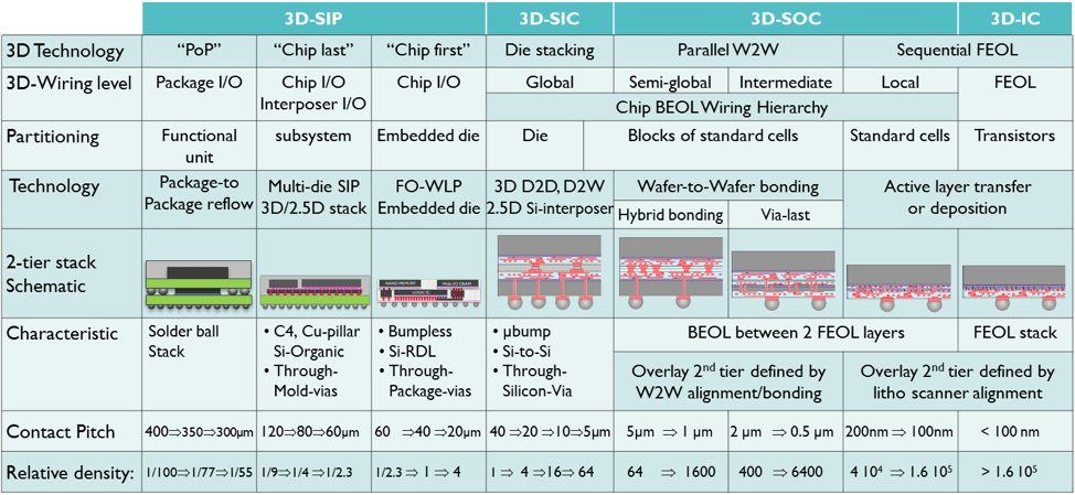
In this 3D technology landscape, several classes of 3D integration can be defined. The main difference between these classes is related to the level of partitioning, in other words: at which level in the interconnect hierarchy the systems are ‘cut’ into different pieces. Each of these classes requires different process schemes and 3D integration techniques, achieving progressively smaller contact pitches. A first class is what we call system-in-a-package (SiP), where the partitioning is done at package level by stacking packages on top of each other, or by integrating multiple dies in a single package. Among the technologies used to realize SiPs are package-to-package reflow and fan-out wafer level packaging FOWLP), in combination with solder balls. Contact pitches of current solutions are rather coarse, in the 400µm range. Imec’s research into new approaches to FOWLP intends to increase the interconnectivity of this class of SiP by a factor 100, targeting interconnect pitches of 40µm. The technique is applied, for example, in mobile applications such as smartphones.
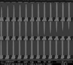
In a second class, called 3D stacked IC (3D-SIC), the partitioning is done at die level and individual dies are stacked on top of each other. 3D-SIC partitioning is achieved using die-to-interposer stacking or die-to-wafer stacking, where finished dies are bonded on top of a fully processed wafer. Dies are interconnected using through-Si vias (TSVs) and micro-bumps. In the industry, micro-bump pitches down to 40µm are achieved today. Imec’s research goal is to bring this pitch down well below 20µm, as such increasing the interconnectivity by one to two orders of magnitude (Figure 1). A typical application example is wide I/O memory, where vertically stacked DRAM chips (3D-DRAM) are connected on a Si interposer together with a logic die and an optical I/O unit.
3D systems-on-chip: higher density through heterogeneous integration
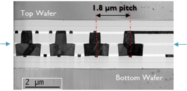
With advanced CMOS scaling, new opportunities for 3D chip integration with even higher interconnect densities and smaller pitches arise. Rather than realizing a SOC as a single chip, it has now become possible to realize different functional partitions of a SOC circuit. Stacking such partitions results in a so-called 3D SoC. These are packages in which partitions with varying functions and technologies are stacked heterogeneously, with interconnect densities below 5µm. The system partitioning can be done at different levels of the interconnect hierarchy – at the global wiring level (long wires, cross chip), intermediate wiring level, or local wiring level (short wires, interconnecting e.g. intra-core modules). The main technological approach to stack these partitions is wafer-to-wafer bonding – either through hybrid (via middle) wafer-to-wafer bonding or dielectric (via last) wafer-to-wafer bonding techniques. This is achieved by aligning the top and bottom wafers that are then bonded. Recently, excellent results in wafer-to-wafer overlay accuracy have been obtained, for both hybrid bonding (1.8µm pitch) and dielectric bonding (300nm overlay across wafer). An accurate overlay is needed to align the bonding pads of the stacked wafers and it is essential to achieving a high yield (Figure 1).
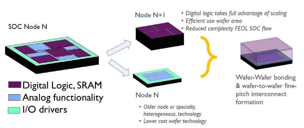
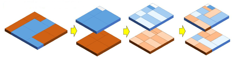
One of the main drivers for 3D-SOC development is functional repartitioning of high-performance systems. In such approach, different parts of the SOC system are realized using tailored technologies in different physical layers but remain tightly interconnected. The trend in processor development, for example, has been towards an ever increasing number of cores. This trend will continue, enabled by the scaling towards 7nm and 5nm technology nodes. More cores will however also need more on-chip memory. And all this will result in more overall silicon area and more back-end-of-line needs – and hence, in an increasing wafer cost. One way to cope with this trend is by functional repartitioning of the processor followed by heterogeneous 3D integration (Figure 2).
Power, performance, area and cost benefits through clever partitioning
The imec researchers use physical design tools to find an optimal 3D functional partitioning of high-performance systems. A typical example is a larger SOC which consists of many cores, L1 memories associated with these cores and L2 memory that is shared. This can be ripped up so that all the memory is brought to a top die, and the logic to a bottom die. We now end up with two dies, half the size of the original big die. And this significantly improves the system’s yield (defined as the percentage of good dies on a wafer) which decreases as a function of the die’s area. In addition to this cost and area gain, the length of the wires between the processor and the memory becomes significantly shorter after stacking the two dies, giving an additional gain in power and performance. These gains are typical for anything that is 3D. But there is more. For the original 2D die, the wafer manufacturing process needs to be optimized for both logic and memory technologies. By splitting the die into two dies, one for logic, one for memory, the processes can be tuned for logic and memory separately. And this will further improve the yield. Also, logic typically requires a large number of metal layers (typically 12 to 14), while memory typically requires fewer layers (5 or 6). This implies that the wafer containing the memory part can now be made relatively cheap – as the back-end-of-line cost makes up a large part of the total wafer cost.

Stacking chips using 3D heterogeneous integration from imec on Vimeo.
In a next step, the partitioning can be revised by making even smaller functional IP blocks and rearrange them into another shape that would further reduce the wire length. The (re-)partitioning should, however, be done in a clever way, avoiding over-partitioning. For example, if a circuit consists of subcircuits that are extremely interconnected, ripping them apart may result in too many wires that go up and down between the two resulting dies. And that would cause more problems than solving anything. A clever way of partitioning may, for example, be based on the scalability of the different technologies. While we keep on scaling transistors according to Moore’s Law, it gets more and more difficult to get an overall process which encompasses everything of the SOC. For these applications, partitioning in function of scalability turns out an interesting solution. If you split the technology into parts that highly scale (e.g. digital blocks) and parts that hardly scale (e.g. analog blocks and I/O drivers), you can optimize the die with highly scalable technologies separately from the die containing less scalable technologies (Figure 3).
Further down the road: 3D-ICs
Eventually, the roadmap will lead to even tighter integration, by stacking transistors on top of each other, achieving contact pitches as small as (a few) 100nm. Imec explores ways of stacking for example nMOS transistors on top of pMOS transistors – or vice versa – instead of putting them next to each other – also known as CFET (or CMOS FET). This, however, involves a completely different technology. It is not about through-silicon-via-like processes: it will be realized through sequential processes or layer transfer processes. The alignment of the two transistors in a CFET should not be wafer alignment defined but lithography defined. A typical application is an SRAM cell in a 3D format, which will have a much smaller footprint than its 2D equivalent. Another example is 3D NAND technology, where a single channel contains multiple transistors or bits (up to 58), integrated into one single structure. So it is a few levels of granularity lower than 3D-SOC partitioning. It is surely one of the future paths with a potential to extend Moore’s law scaling.
3D-SOCs and 3D-ICs complete imec’s 3D technology roadmap that outlines different paths for 3D integration. However, imec researchers refer to a ‘3D technology landscape’ instead of a ‘roadmap’. It is not like a clear traditional roadmap that can be read from left to right. For 3D, there are a lot of technology options that will coexist, even within the same system. The technologies differ in where they intercept the hierarchy of interconnects on the chip, in other words, where we cut the devices and make the 3D interconnectivity. And this will determine the required 3D pitch. So it is more like a collection of technologies that allow a system to be integrated into a much smaller form factor, with increased performance and lower manufacturing cost.