
In early April the Defense Industrial Base Consortium (DIBC) held an “Industry Day for Advanced Printed Circuit Boards (PCBs) and Electronic Substrates” at the IPC APEX Expo.
Let’s look at the “Advanced Printed Circuit Boards and Substrates Industry Day” presentation by

Korine Duval, Ph.D., Microelectronics Sector Lead for the Innovation Capability and Modernization office.
Many of you have shared with me that you appreciate seeing how the different departments of the U.S. Government interrelate, especially since many of them have started financially supporting advanced packaging.
Figure 1 depicts the technology readiness level (TRL) supported by various US Government programs.
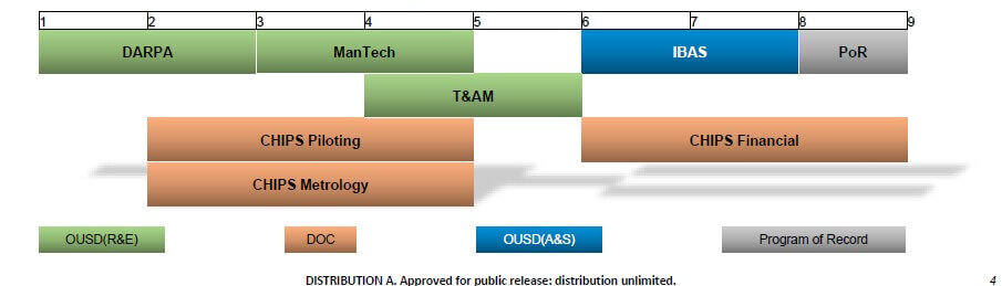
- OUSD (R&E) = Office of the Under Sect of Defense (Research & Engineering)
- OUSD (A&S) = Office of the Under Sect of Defense ( Acquisition & Sustainment)
- DoC = Dept of Commerce
While most of you have heard of DARPA and ManTech, you’re probably less familiar with Trusted & Assured Microelectronics (T&AM), which, for instance. is the home of the SHIPS, STEAMPIPE, and STAMP programs. We also see that T&AM and IBAS are both divisions of OUSD.
Defense Industrial Base Consortium (DIBC)
Mission:
To coalesce and expand the defense industrial base (DIB) in support of the Manufacturing Capability Expansion & Investment Prioritization (MCIEP) critical subsectors. MCIEP is focused on addressing defense supply chain issues, developing the industrial workforce, sustaining critical production, commercializing R&D efforts, and rapidly scaling emerging technologies to build a robust, resilient DIB.

Critical Sectors:
Kinetic capabilities (hypersonics), energy storage and batteries, microelectronics, castings & forgings, strategic and critical materials, and workforce development.
Vision:
To deliver a resilient US supply chain and workforce able to respond in times of national security crisis without reliance on foreign sources.
Advanced PCBs and Substrates
Technical Element 1: Ultra high-density Interconnects & Organic Integrated Circuit Substrates
- Prototype the development of domestic sources for PCBs and/or organic IC substrates that have approximately ≤75μm microvias, ≤50μm traces and spaces, and ≤50μm dielectric thickness and expand domestic capability and capacity to produce such products. This can include investments in prototyping various semi-additive process capabilities and capacities, building on those delivered by traditional subtractive processes.
- Reliable medium volume 25-65 μm lines/spaces
- High reliability in ≥ 3 layers of stacked microvias
- BGA pitch ≤ 0.3 mm
- High-frequency applications (50 Ghz and above)
- Industrial standards for high-reliability applications of UHDI products (design and performance)
- Reliability data to support new designs and materials
- Facilities, Equipment, Materials and Processing
- Clean rooms / minimize particulates in air, chemistry, equipment
- Automated material handling throughout manufacturing
- Laser drill < 50 μm diameter capability
- Direct imaging <= 20 μm line and space capability
- AOI capability <= 20 μm line and space capability
- Electrical test <= 0.3 mm pitch capability
- Specialized via fill plating equipment
- Advanced materials
- Thin copper foils, advanced laminates, build-up films, thin electroless copper, high-resolution photoresists, via fill chemistry, low etch rate oxide and etching, high-resolution solder masks
- Semi-additive processes (SAP) and modified SAP (mSAP)
Technical Element 2: Domestic Sourcing for Enabling Materials for Manufacturing
- Prototype state-of-the-art capabilities to enable the development of advanced materials for DoD applications (copper foils for modified semi-additive applications, build-up film equivalents, advanced laminates for organic IC substrates, and solder masks for organic substrate applications.)
Technical Element 3: Improved Microvia Reliability
- Prototype new models for improving microvia reliability across various manufacturing sources. Develop and validate design rules and process parameters that yield stable/reliable results on current and emerging HDI, UHDI, and/or organic IC substrate technologies. This could involve a detailed design of experiments (DOE) involving printed board designers, manufacturers, process equipment, chemistry, and materials suppliers
Technical Element 4: HDI/UHDI Reliability Data
- Develop and prototype standards and test methods that assess the reliability characteristics of design rules, materials, and processes for HDI, UHDI and/or organic IC Substrate features. Other prototyping and test efforts could include sponsored and comprehensive highly accelerated stress testing of HDI and UHDI structures to assess long-term operational reliability in high-stress environments. Test requirements should be incorporated into relevant industry and DoD requirements and documents.
The U.S. Government is accepting proposals for Advanced PCBs and Substrates based on these elements and will perform technical evaluations of all that are submitted. If selected for an award, the submitter will be asked to provide a statement of work (SOW) and cost proposal.
For all the latest in Advanced Packaging, stay linked to IFTLE


