

TSMC Off-shore Production
Digitimes reports that when it comes to the production capacity of 28nm and below, TSMC has stated that within five years, the ratio between Taiwan-based vs overseas production capacity will be 80/20.
TSMC has already planned six manufacturing sites with the announcement of 5nm Fab 21 in Arizona. In November 2022, TSMC founder Morris Chang publicly announced that Fab 21 would advance to 4nm. Then, at the launch ceremony of TSMC’s Arizona plant in December 2022, it was announced that TSMC’s 3 nm technology, which had not yet been mass-produced in Taiwan at that time, would be transferred to Fab 21 “in the future”.
In late December, TSMC held a 3nm mass production and expansion ceremony at Fab 18 in Taiwan. TSMC has secured customers like Apple, while Samsung still hasn’t revealed who their customers for 3nm are. Even the yield rate remains undisclosed.
Some in Taiwan feel that the speed of exporting TSMC’s advanced technology to the US seems to be accelerating, which has generated heated discussions.
TSMC’s recent earnings call has stated that within 5 years (i.e. 2027) the 80/20 production capacity of sub-28nm process nodes will be in place. This offshore production includes not only the US, but also Japan where TSMC has started building factories, and Europe where TSMC is negotiating.
Why 2027?
Digitimes postulates that this is related to the fact that the US released the ‘National Security Strategy‘ report in October 2022, and the US DoD released the ‘China Military Power Report‘ in late 2022, which reported that the Communist Party of China (CPC) expects to achieve certain economic/military goals by the year 2027. U.S. officials added that if China achieves its 2027 goals, it will have sufficient capabilities to unify Taiwan by force.
TSMC to Build Further Factories in Japan and Europe
Asia Times reports that TSMC is likely to build a second factory in Japan and is moving toward building one in Europe as well.
Like the US, Japan and the EU have both pursued investment from TSMC. “We are also considering building a second fab in Japan as long as the demand from customers and the level of government support make sense.” Asia Times reports that Japan is short of foundry capacity and government subsidies will almost certainly be forthcoming given how much more expensive it is to build in Japan compared with Taiwan.
That’s the approximate size of the grant the Japanese government has offered for the specialty technology fab that Wei mentioned. Called Japan Advanced Semiconductor Manufacturing, it is a joint venture between TSMC, Sony, and Toyota affiliate, Denso.
Its products will reportedly include image sensor data signal processors, automotive ICs, and other logic devices, with priority on supply to Sony, Denso, and other customers in Japan. Sony is the world’s top maker of image sensors.
The size of the Japanese subsidy is reportedly in line with statements made by TSMC executives regarding the cost of production in the US. In April 2022, TSMC founder Morris Chang said that “manufacturing chips in the US is 50% more expensive than in Taiwan.”
TSMC reports that the major reason for the cost gap is the construction cost of building and facilities, which can be 4 to 5 times greater for a US fab versus a fab in Taiwan… “The high cost of construction includes labor cost, cost of permits, cost of occupational safety and health regulations, inflationary costs in recent years and people and learning curve costs.”
Construction and other costs in Japan are also high, and despite concerns about return on investment, attracting TSMC’s expertise and building new and more advanced semiconductor production capacity are top national priorities.
According to the SIA (report issued in September 2020), “Depending on the type of fab, a new fab in the US costs approximately 30% more to build and operate over 10 years than one in Taiwan, South Korea, or Singapore, and 37-50% more than one in China. As much as 40-70% of that cost differential is directly attributed to government incentives.”
Japan is also in the process of building up its own semiconductor foundry industry. Last August, Sony, Denso and six other Japanese companies established a joint venture called Rapidus to build advanced logic foundry capacity in Japan.
A second TSMC fab would help TSMC avoid losing market share to Japanese reshoring of production now outsourced to Taiwan.
If a decision to build is made this year, it might come online as early as 2025. Rapidus is targeting production at the 2-nanometer node in 2027, two years after TSMC.

In Europe, TSMC is “engaging with customers and partners to evaluate the possibility of building a specialty fab focusing on automotive-specific technologies based on the demand from customers and level of government support.”
To build this fab, TSMC will probably require a subsidy similar to those it has been offered in Japan and the US.
TSMC began installing equipment at its new fab in Arizona in December. Investments in Japan and Europe will probably follow, but TSMC is likely to be cautious about the timing.
STEAM PIPE
The DoD SHIP program looks to bring in new players in 2023 (beyond current participants Intel, Qorvo, and Mercury Systems). They will do this through their new program, STEAM PIPE.
STEAM PIPE stands for Strategic Transition of Microelectronics to Accelerate Modernization by Prototyping and innovate in the Packaging Ecosystem. Yes, I agree, from now on we will simply use the acronym.
S2MARTS, the Strategic & Spectrum Missions Advanced Resilient Trusted Systems, is the DoD’s contracting vehicle for acquisition in trusted microelectronics, strategic and spectrum missions, and other critical mission areas. Figures 1-3 provide more details on these programs.
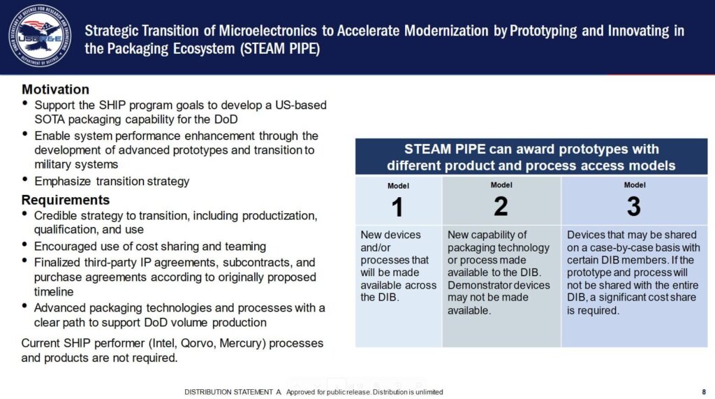
 Packaging must be performed in North America or Europe. Asian-sourced materials, IP, and processes must be explained and justified. Packaging technologies and processes must have a clear path to support DoD volume production.
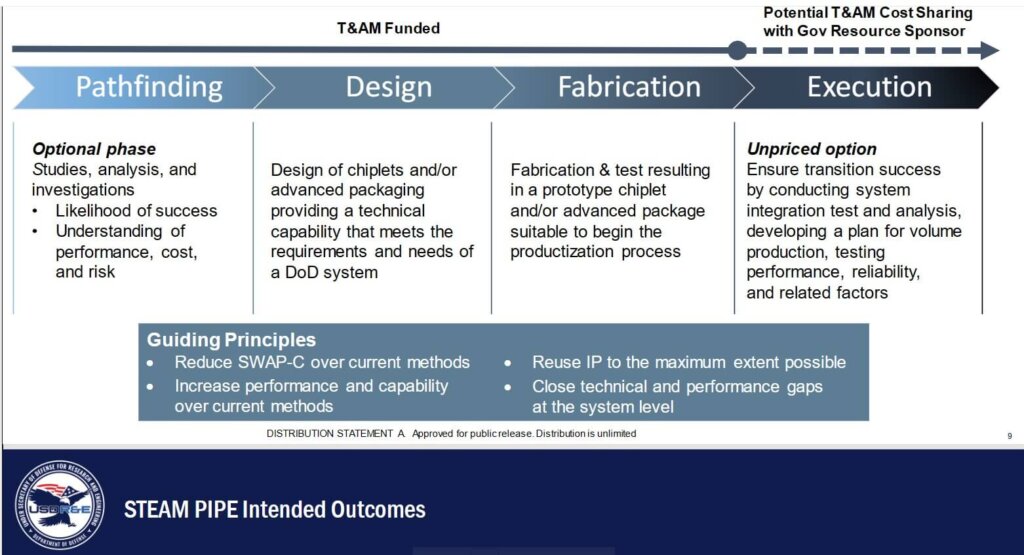
- Each award must be completed within 5 years—preferably phase 1 in 36 months or less and phase 2 in 24 months or less.
- The total project budget from the T&AM SHIP program for STEAM PIPE is $60MM (subject to change).
For all the latest in Advanced Packaging stay linked to IFTLE……………………


