

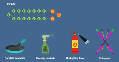
From November to April for the past seven years, I have spent a considerable amount of time on the snow as a ski instructor. In 2019 the International Ski and Snowboard Federation implemented a ban on fluorinated waxes that took place in July of 2021. The change left skiers scrambling, as while there were other waxing alternatives, the addition of polyfluorinated alkyls (PFAS) to the ski wax helps to make them hydrophobic. The PFAS also adheres better to the ski through the length of the race as they take a longer time to break down. The ban has been in full place since 2021.
Just recently Norway’s Ragnhild Mowinckel was disqualified as her skis tested positive for fluorinated wax after the first run. The contamination appears to have been caused by a waxing tool; however, there have also been comments about the quality of the wax testing and other ways the skis could have been inadvertently contaminated.
I use the above example to demonstrate how PFAS has many uses, and it will be extremely challenging to unwind its use in our daily lives let alone the semiconductor industry as Figure 1 shows.
The semiconductor industry, like the ski industry, is facing challenges with PFAS. While there have yet to be outright bans on the use of PFAS such as in the racing part of the ski industry, the semiconductor industry is highly dependent upon the use of PFAS in many parts of the manufacturing of semiconductors, from the plastic containers used to transport chemicals to piping in the fab, chiller fluids, and coatings inside process equipment.
SEMI has been active in working with governments worldwide on managing the use of PFAS in the semiconductor process and working to help educate policymakers on how critical PFAS are in the making of semiconductors, and a great deal of study needs to go into how to manage and protect the environment from PFAS. One of the semiconductor industry concerns is that unless sufficient time is given to developing alternatives, is that the semiconductor industry could be shut down if broad bans are put into place.
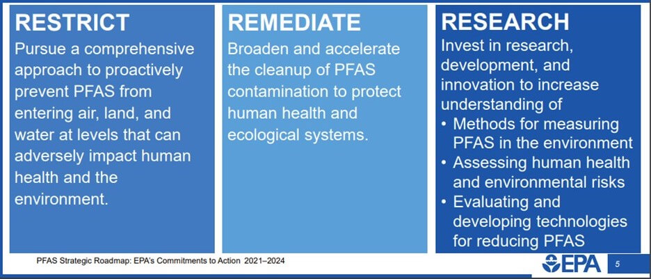
In January of 2024, SEMI held a briefing where the EPA shared its progress on PFAS research and regulations. The EPA Council on PFAS was established in April of 2021, so only a short time ago. An area of key focus is to restrict, remediate, and research.
A great deal of the presentation was focused on the progress that the Council on PFAS has made on methods, reporting and regulations. One of the challenges for the U.S. is that based upon the SEMICON West seminar on PFAS presented by Kevin Fay, Executive Director of Sustainable PFAS Action Network (SPAN), more than 330 PFAS bills have been considered at the state level since 2021, and 12 states have instituted product bans.
Going back to the skiing example, the state of Vermont has banned the use of fluorinated wax in the state since 2021. The EPA in 2023 banned the import of fluorinated wax. Other states and ski areas are working to phase out fluorinated wax as PFAS are showing up in the local water supplies.

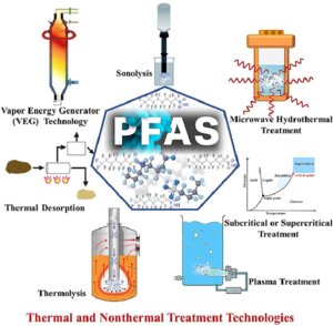
Identifying the source of PFAS in the semiconductor industry is the easy part of the problem. In some cases, such as the photoresist process, they are considered critical materials, and an alternative solution has yet to be created. Thus, the industry needs to find ways of breaking down the PFAS into their elemental forms. The EPA seminar provided a link to this article. The paper concluded that there is still a lot of work to do to find an effective economical solution (Figure 3).
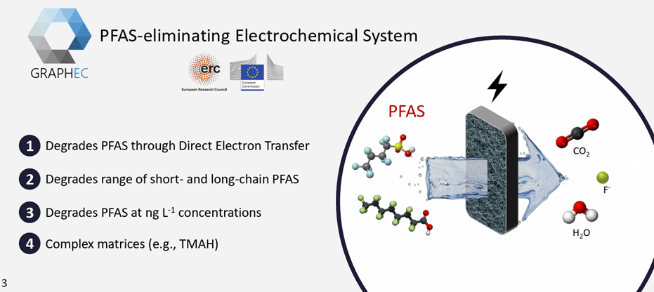
However, at SEMICON West 2023, during the SEMI Sustainability Startup Forum, Graphec demonstrated a lab-scale solution and was building a prototype system that degrades the PFAS through direct electron transfer.
Prototype work is scheduled to be completed at the end of 2024, so if the system is as successful as the lab tests, hopefully, it can be scaled up and connected to the waste stream of a fab, if it is successful there then can it be expanded at a larger scale.
While elimination from the waste stream is one option, finding alternatives that easily find their way into the waste stream is another. Just as the semiconductor industry has found solutions to toxic must-have chemistries of the past, it needs to do the same with PFAS. Fortunately, SEMI is taking a proactive role as an industry advocate in looking for a solution using both options.

