PulseForge, an industry pioneer specializing in advanced solutions for the semiconductor sector, is spearheading efforts to drive the global adoption of 2D materials in devices and packages using its photonic debonding technology for successful 2D material transfer.
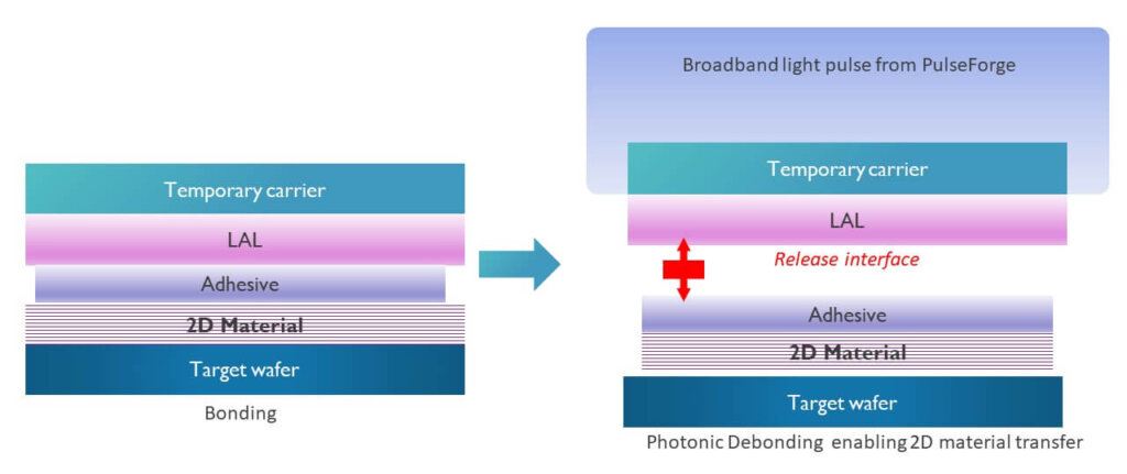
PulseForge is on a mission to transform the semiconductor industry by harnessing the unique properties of photonic debonding to enable defect-free 2D materials transfer from the growth substrate to the target substrate, which is useful for the range of layered, crystalline van der Waals materials including graphene, Xenes, and MXenes (Figure 1).
In a strategic move, PulseForge is excited to partner with imec, a global leader in nanoelectronics and digital technologies research, to accelerate the adoption of 2D materials for next-generation electronic devices.
As a notable outcome of this strategic partnership, imec, and PulseForge have successfully demonstrated extremely clean transfer of 2D materials on a 300 mm wafer scale with minimal residue and over 99.5% transfer yield, propelling the integration of these materials into electronic devices and systems. The initial findings of this work were presented at the IMAPS Symposium in October 2023. This collaboration also enables imec researchers to pursue sequential TMDC layer transfer for stacked nanosheet applications.
2D material transfer has long been a barrier to industrial adoption, which is well-stated in the 2022 Nature review from Liu et.al “Highly uniform large-area transfer necessitates an ultraclean interface with minimum residues or defects over a 12-inch area, which represents a formidable challenge.” As showcased at the 2023 IMAPS Symposium, the collaborative work between PulseForge and imec, demonstrated the transformative potential of photonic debonding in facilitating the clean, high-yield transfer of 2D materials over large areas.
To further solidify this partnership, the state-of-the-art PulseForge PD300 SA, a photonic debonding tool, will be installed at imec’s cleanroom facility in Leuven, Belgium. This installation serves as a testament to the unwavering commitment of both organizations to push technological boundaries and foster innovation in the realm of 2D materials.

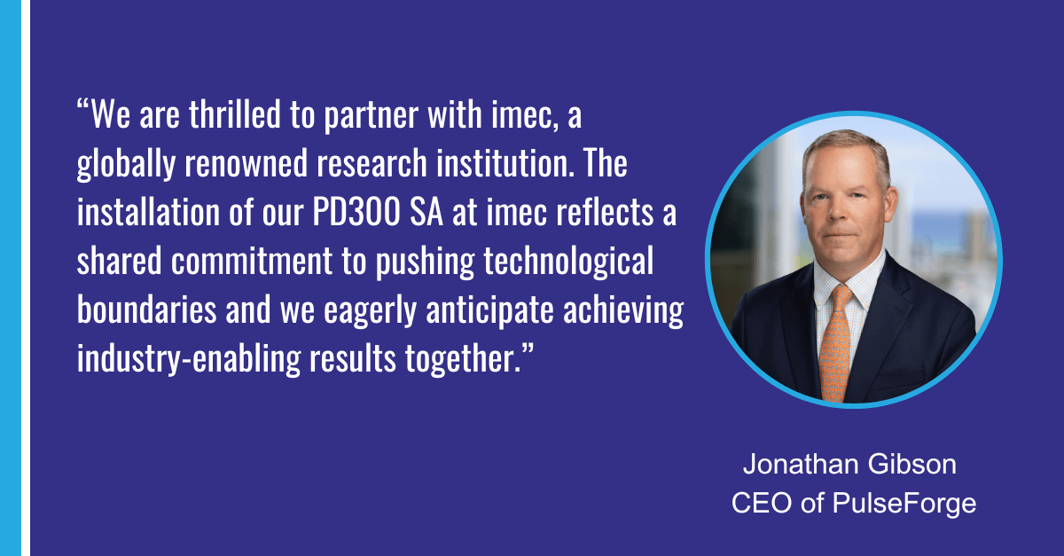
Mr. Jonathan Gibson, CEO of PulseForge, expressed his enthusiasm, stating, “We are thrilled to partner with imec, a globally renowned research institution. The installation of our PD300 SA at imec reflects a shared commitment to pushing technological boundaries and we eagerly anticipate achieving industry-enabling results together.”
As PulseForge continues to push the boundaries of innovation, the company remains poised to shape the future landscape of the semiconductor industry. Through ongoing research, development, and collaboration, PulseForge is committed to driving meaningful progress and driving the adoption of 2D materials worldwide.
References:
[1] Liu, Y., Duan, X., Shin, HJ. et al. Promises and prospects of two-dimensional transistors. Nature 591, 43–53 (2021).