
WILMINGTON, Mass.–(BUSINESS WIRE)– Onto Innovation Inc. (NYSE: ONTO) today announced the introduction of the Atlas® S optical critical dimension metrology system and the Element™ S high-speed impurity mapping, dielectric film composition and epi thickness measurement system. The two new systems complement existing Dragonfly® inspection, IVS™ overlay, and Echo™ metrology product families building on the company’s strategy to provide a portfolio of comprehensive process control tools and software that work together to solve a wide range of inherent process challenges in the specialty markets. Within the specialty markets, growth of power applications, based on Si, SiC and GaN device technologies, is fueled by the transition to electric vehicles and the rapid adoption of GaN into fast charge applications in both consumer and automotive markets. Specifically, the demand for SiC and GaN power devices is seeing an annual average growth rate approaching 34% and 44% respectively, through 2027, according to Yole Group. Customer enthusiasm around both Atlas S and Element S systems has resulted in over $26 million in bookings with customers taking delivery of initial systems in the fourth quarter of 2023. These new systems, along with the entire Onto specialty portfolio, contribute to a 24% increase in year over year revenue for Onto in the power device market.
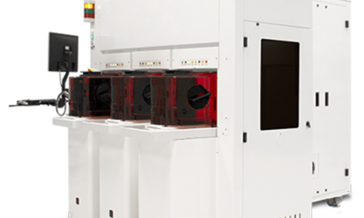
The Atlas family of products, including the 2022 Best of West winner Atlas V system, has been previously adopted by top DRAM, NAND and logic manufacturers for both optical critical dimension (OCD) metrology and planar films applications. The breadth of capabilities and productivity of the Atlas S system are well suited to a broad range of specialty applications. “With the complexity of automotive power and specialty devices increasing and the ongoing wafer size migration, metrology requirements are getting tighter. Equipped with the latest-generation compute and model guided-machine learning abilities, the Atlas S system enables OCD metrology leveraging Mueller matrix-based analysis and Onto Innovation’s Ai Diffract™ modelling engine, making it a powerful and flexible optical metrology tool capable of addressing current and future market needs,” says Aditya Vyas, vice president of business development for Onto Innovation.
Currently expanding into the power device and broader specialty markets, the Element product family uniquely combines transmission and reflection mode-based Fourier transform infrared (FTIR) measurement systems and has been successfully implemented in DRAM and CIS manufacturing. “Multi-layer epitaxial layer modeling is important for many new optical, MEMS and power devices. The Element S system provides excellent precision in epi layer characterization using advanced modeling to accurately measure thickness and free carrier concentration in up to five epi layers to the very edge of 100mm to 200mm wafers in Si, SiC and the variety of specialty devices where epi layers are becoming more integral to device performance,” says Mike Rosa, Onto’s chief marketing officer and head of strategy. “With improved precision, the Element S system offers lower cost of ownership and higher throughput compared to legacy products.”
With a variety of device types, materials and complex structures, the specialty market brings many unique challenges to film and dimensional metrology that are distinct from those found in the advanced node applications. Onto’s flexibility in addressing these challenges both individually and as part of a broader portfolio of metrology, inspection and enterprise software products positions the company to better support customers in this rapidly growing and increasingly diverse space.
To learn more about Onto’s specialty portfolio products, visit Onto Innovation during SEMICON® West at booth 629 to discuss metrology applications or reach out to your local sales team to learn more about the Atlas S or Element S metrology systems.

About Onto Innovation Inc.
Onto Innovation is a leader in process control, combining global scale with an expanded portfolio of leading-edge technologies that include: Un-patterned wafer quality; 3D metrology spanning chip features from nanometer scale transistors to large die interconnects; macro defect inspection of wafers and packages; metal interconnect composition; factory analytics; and lithography for advanced semiconductor packaging. Our breadth of offerings across the entire semiconductor value chain combined with our connected thinking approach results in a unique perspective to help solve our customers’ most difficult yield, device performance, quality, and reliability issues. Onto Innovation strives to optimize customers’ critical path of progress by making them smarter, faster and more efficient. With headquarters and manufacturing in the U.S., Onto Innovation supports customers with a worldwide sales and service organization. Additional information can be found at www.ontoinnovation.com.


