

The IPC is a non-profit global association for printed circuit board (PCB) manufacturers. Traditionally its focus has been on printed wiring boards, but more recently, as high-density PCB substrates have been used in packaging applications like BGAs, they have entered the realm of advanced packaging. Based on the announcements of the US “on-shoring” efforts and the expected monies that will be made available to achieve these goals, this past fall (2021) IPC issued a report entitled “North American (NA) Advanced Packaging Ecosystem Gap Assessment”. They claim their market data is accurate as of 2Q 2021. IPC lists the sources for this report as 2021 SIA databook, TechSearch International, and Prismark Partners.
So…let’s take a look at what the gap assessment report concludes. I have inserted comments when I disagree with their conclusions.
Gap Assessment Report Critical Market Segments
IPC identifies critical market segments as systems and products that are required for national security. They include:
- Defense/aerospace and space electronics
- High-performance computing (HPC)
They conclude that these two market segments in NA account for $90B in sales.
They conclude that today’s packaging and electronic component advancements do not come from the mil/aerospace/defense community. Next-generation advancement generally comes from (a) HPC systems and (2) consumer electronics. Thus, integration of the latest technologies into the defense/aerospace sector tends to lag SOTA adoption in commercial segments and products.
Defense, Aerospace and Space Electronics
Products for this market segment are critical to national security. Applications can be defined by application (communications, search and navigation, avionics, etc.) The total defense market is estimated to be $38B/yr.
IPC states that “America’s defense electronics supply chain is dangerously thin and falling behind due to the commercial offshoring of American manufacturing…. We have spent the last 20+ years educating other countries on how to build products we need. Now they have started to exceed our remaining internal capability.”
High-Performance Computing (HPC)
HPC is the backbone of critical infrastructures such as financial banking, the stock exchange, retail commerce, mobile communications, government, power distribution, and national security/defense. The HPC market in NA was estimated to be ~$30B in 2020.
Semiconductor Fabrication
Building an entry-level manufacturing plant for 50K wafers/month today costs ~ $15B. This means very few companies can afford to keep up. For perspective, GlobalFoundries and UMC stopped moving to the next node at 28nm.
NA semiconductor companies have largely migrated to a fabless model meaning we can design the next generation chips but are heavily dependent on Asian supply for chip manufacturing, IC substrate production, and IC packaging. Key US fabless companies include Qualcomm, Broadcom, Nvidia, AMD, and Apple.
While this has been a successful business model, it places companies in a difficult long-term position of being unable to physically produce semiconductor devices.
TSMC and Samsung are manufacturing at the 7nm node and have introduced the 5nm node. Intel has been in the news in recent years as they have fallen behind and are struggling at the 10nm node. Recent reports indicate that TSMC and Samsung are planning 5nm foundries in the US in 2024.
Advanced node foundry capability coming online in the US post-2024 will require matching advancements in substrate and packaging and assembly production.
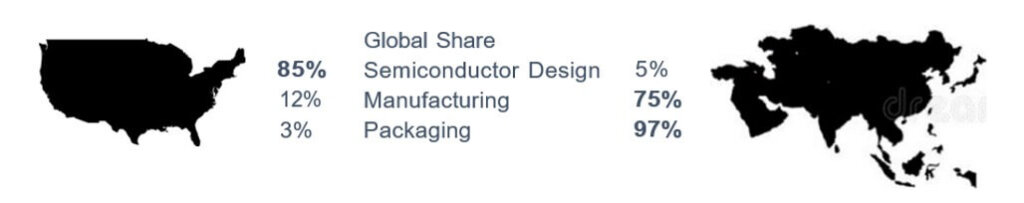
Overall Asian Dominance
“Asian dominance is observed for nearly the entire semiconductor supply chain” with top companies dominating market share across semiconductor fab (TSMC, Samsung), Advanced IC Substrates fab (Unimicron Ibiden, SEMCO, NanYa, Shinko); OSAT assembly and test (Taiwan holds nine of the top spots including ASE/SPIL, Powertech; PCB and EMS (electronic manufacturing services) where offshoring has been the norm for more than 20 years.
IC High-Density Substrates
Regardless of the package type, whether silicon interposer, embedded bridge, fan-out-on-substrate, or RDL interposer, a high-density laminate substrate is used to form the base of the high-performance package. The most complex of these substrates have large body sizes and high layer counts.
FC-BGA substrates with build-up layers are used for CPUs in laptops, desktops, gaming and servers, GPUs and FPGAs for AI accelerators, ASICS for telecom, and media products such as HDTV. Major US companies like AMD, Broadcom, IBM, Intel, Nvidia, Xilinx, and others require advanced FC-BGA substrates to make their products for applications like data centers and telecom. Capacity is being added to meet increased demand, but nearly all of it is in Taiwan, none is in the US. IPC concludes that currently there is no IC substrate capability within NA to produce advanced FC- BGA or FC-CSP substrates.
IPC correctly notes several barriers to entry for advanced substrate reshoring back to the US including:

- $1B investment required
- 20+ yrs of market leader know-how gap
- labor force gap (requires > 1000 workers)
- raw material (like ABF dielectric film) supply not located in the US
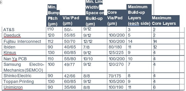
Key global substrate suppliers and their capabilities are shown in Figure 2. Finer features and coreless structures are on these company roadmaps.
Silicon Interposers
This IPC report spends very little time on silicon interposers but does mention that “…major suppliers such as TSMC, UMC, Samsung are located in Taiwan and Korea.” They note there are very few suppliers of silicon interposers in the US, listing GlobalFoundries, Micross, Skorpios (Austin TX), and Skywater in Orlando.
IFTLE’s opinion differs substantially:
- GlobalFoundries appears to supply Si interposers only to customers for whom they are making chips. They have shown no desire to become a merchant source
- Micross does not claim to have a full commercial process in place for Si interposers but is involved with programs to fabricate prototypes doing several process steps at 3rd parties
- Skywater does not have any production capability in place yet in Orlando to commercially manufacture Si interposers Skorpios has not publicly announced any commercial capacity for the production of silicon interposers. I know of no one using them for commercial supply.
To maintain a strong military and aerospace industry a reliable source of bumping, assembly, and test are also necessary.
OSATS
Taiwan has nine different outsourced semiconductor assembly and test (OSAT) companies offering 3rd party IC packaging and test of devices made at foundries, fabless companies, and integrated device manufacturers (IDMs) (Figure 3).
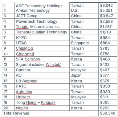
IPC considers the NA OSAT segment “healthy” because they count 25 medium-to-small OSAT companies in NA. Amkor, with headquarters in the US, is the only OSAT in the top 20 and they have no production facilities in the US. (See table 21 “NA OSAT listing” in the full IPC report)
While IFTLE does not disagree that this list contains commercial operations who do assembly, we do not count this segment as “healthy” in terms of advanced packaging and assembly since there are ZERO companies on this list that do the kind of SOTA advanced packaging necessary for chiplets, 2.5D, 3D, silicon or glass substrates, embedded (EMIB), etc.
Bumping
Bumping has traditionally been an OSAT service, but it is also available at major foundries like TSMC. Taiwan accounts for > 40% of global flip-chip bumping including copper pillar and solder bumping. South Korea has 27% and China 16% (Figure 4).
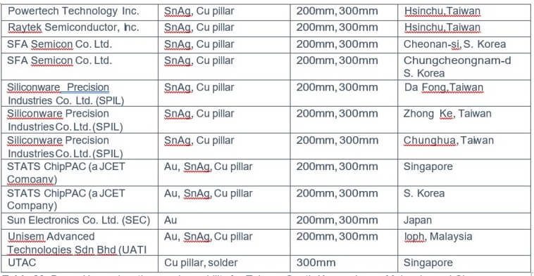
There are also four reported locations in China capable of SnAg and copper pillar and 300mm:
- Huatian, Shanghai
- JCET, Jianglin
- TongFu Miro, Nantong
- Unisem Advanced Technology, Chengdu
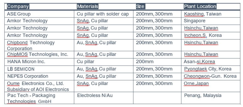
The IPC lists six merchant companies in NA, noting that they have small or prototype capacity and limited 300mm availability (Figure 5).
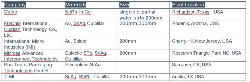
IFTLE is in mild disagreement with this conclusion. The only place merchant 200mm manufacturing supply exists is at Flip Chip International in Phoenix (currently owned by Huatian of China) and Micross, which runs the old Amkor 200mm line in RTP NC.
While players like Intel certainly have their flip-chip capability, they do most of their commercial bumping in Taiwan, not in the USA.
There is NO 300mm merchant bumping capability in the US and that includes China-owned FCI.
If future sub 10nm IC fabs proposed > 2024 by TSMC (Az), Samsung (TX) and Intel (OH) are proposing to include micro bumping capability in these facilities, that certainly would be a good idea but that is not something that is/has been reported thus far.
For all the latest on Advanced Packaging stay linked to IFTLE.


