
Finishing up our coverage of the 2021 IEEE 3DIC conference, we take a closer look at glass embedding, 3D stacked packaging for retinal prosthesis, and the chiplet design exchange.
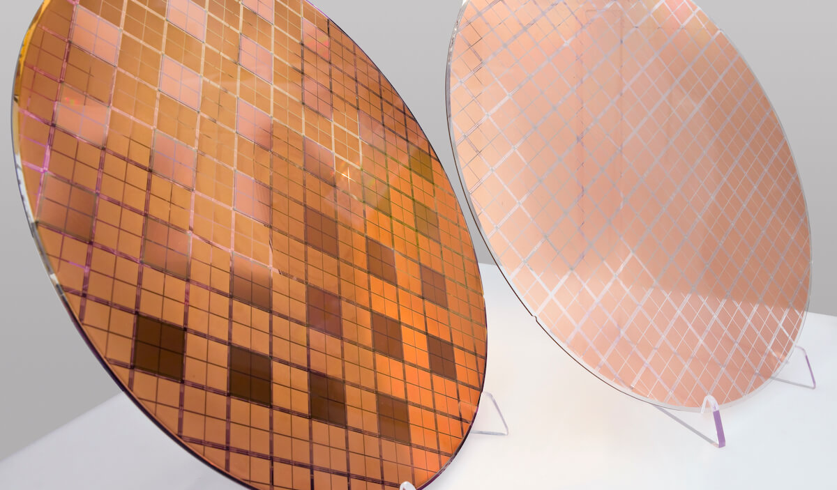
Georgia Tech – Glass Embedding
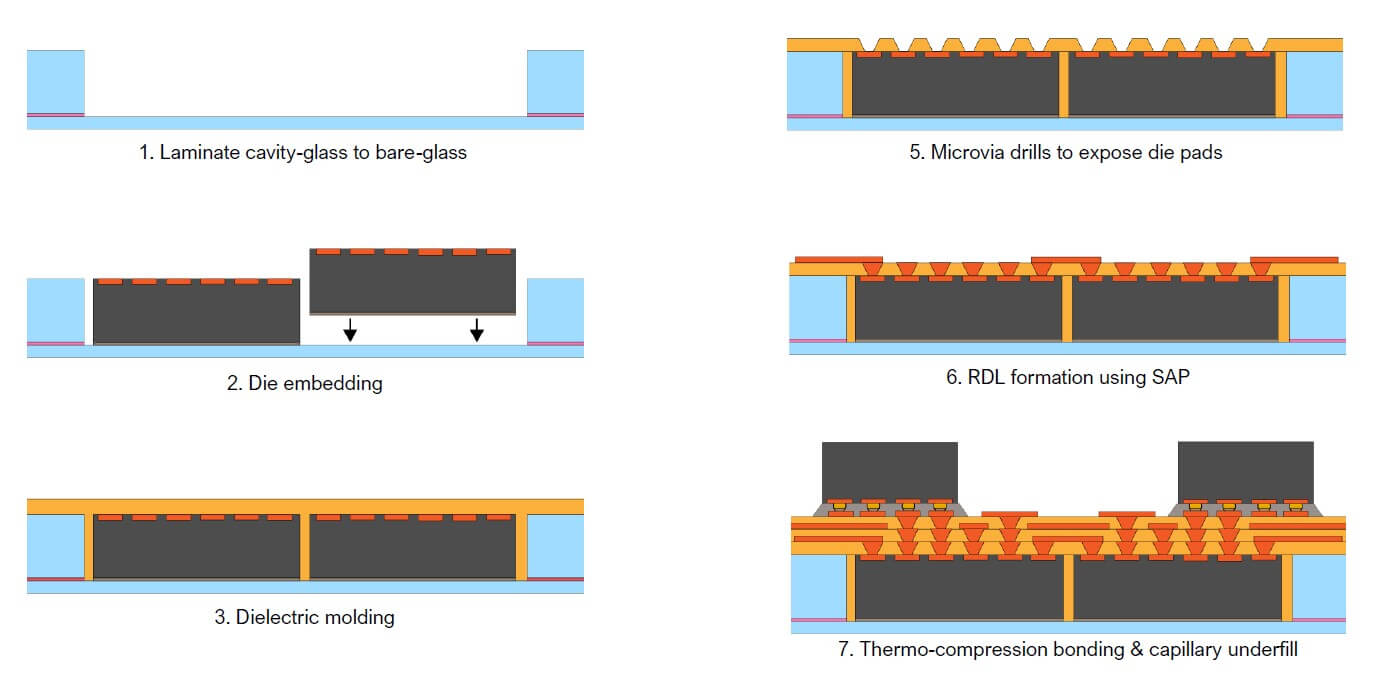
Madhavan Swaminathan, who has replaced Rao Tummala as the Director of the GaTech Packaging Research Center (PRC) discussed 3D Integration, Trends, Challenges and Opportunities. Carrying forward the work the PRC has done with glass substrates over the last decade, Swaminathan showed the following glass panel embedding process flow (Figure 1).
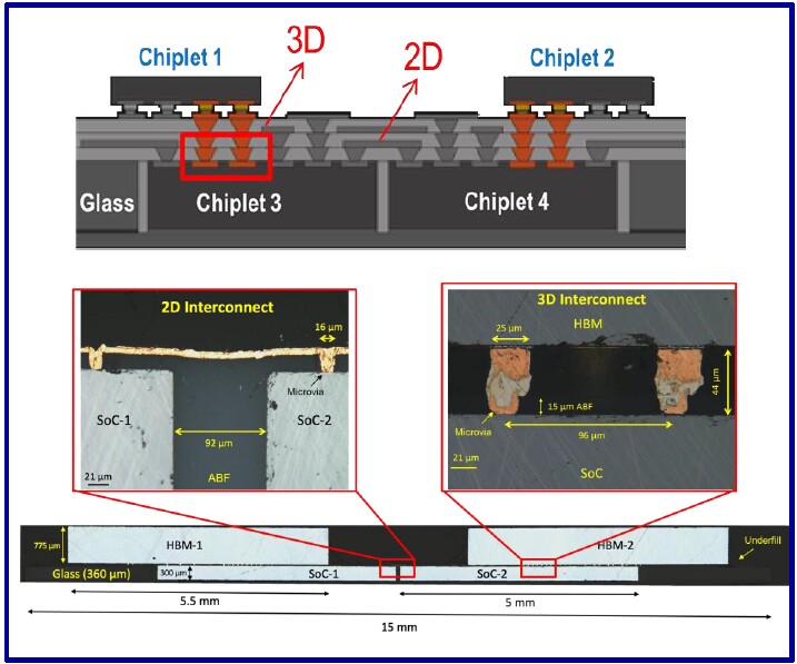
This enables both 2.5D and 3D connections as shown in Figure 2.
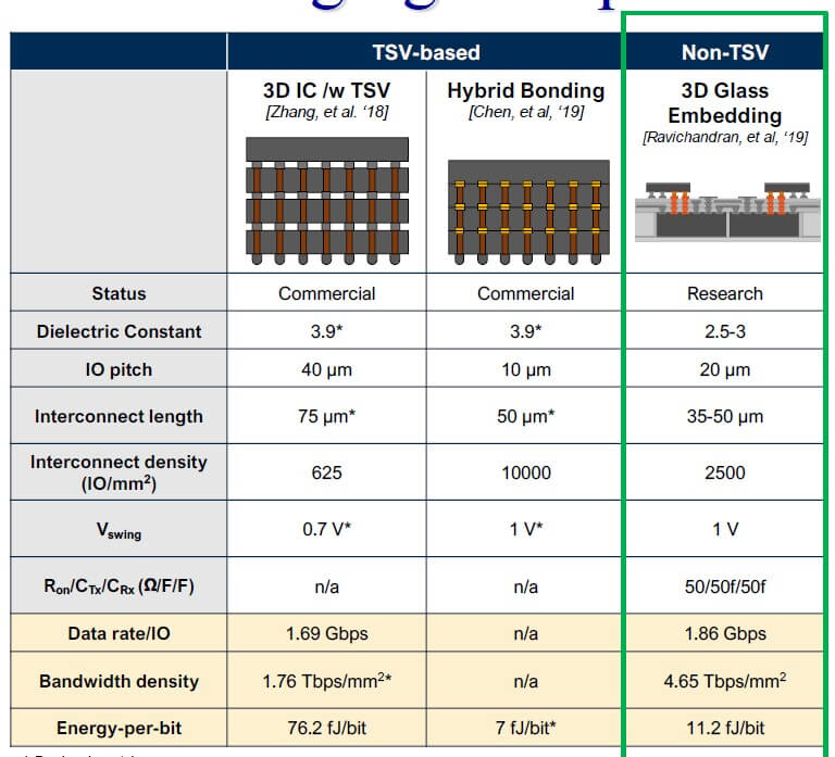
This glass embedding technology is compared to micro bumping and hybrid bonding in Table 1.
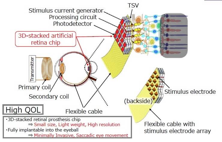
Tohoku University 3D Retinal Prosthesis
Tetsu Tanaka from Tohoku Univ updated the audience on their work to develop a fully implantable retinal prosthesis using 3D-stacked packaging. For those of us who have followed 3DIC technology through the decades, we know that this has been the goal of Mitsu Koyanagi for years.
The concept of the fully implantable retinal prosthesis is shown in Figure 3:
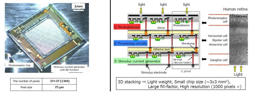
The 3D-stacked retinal chip is shown in Figure 4.
UCSB
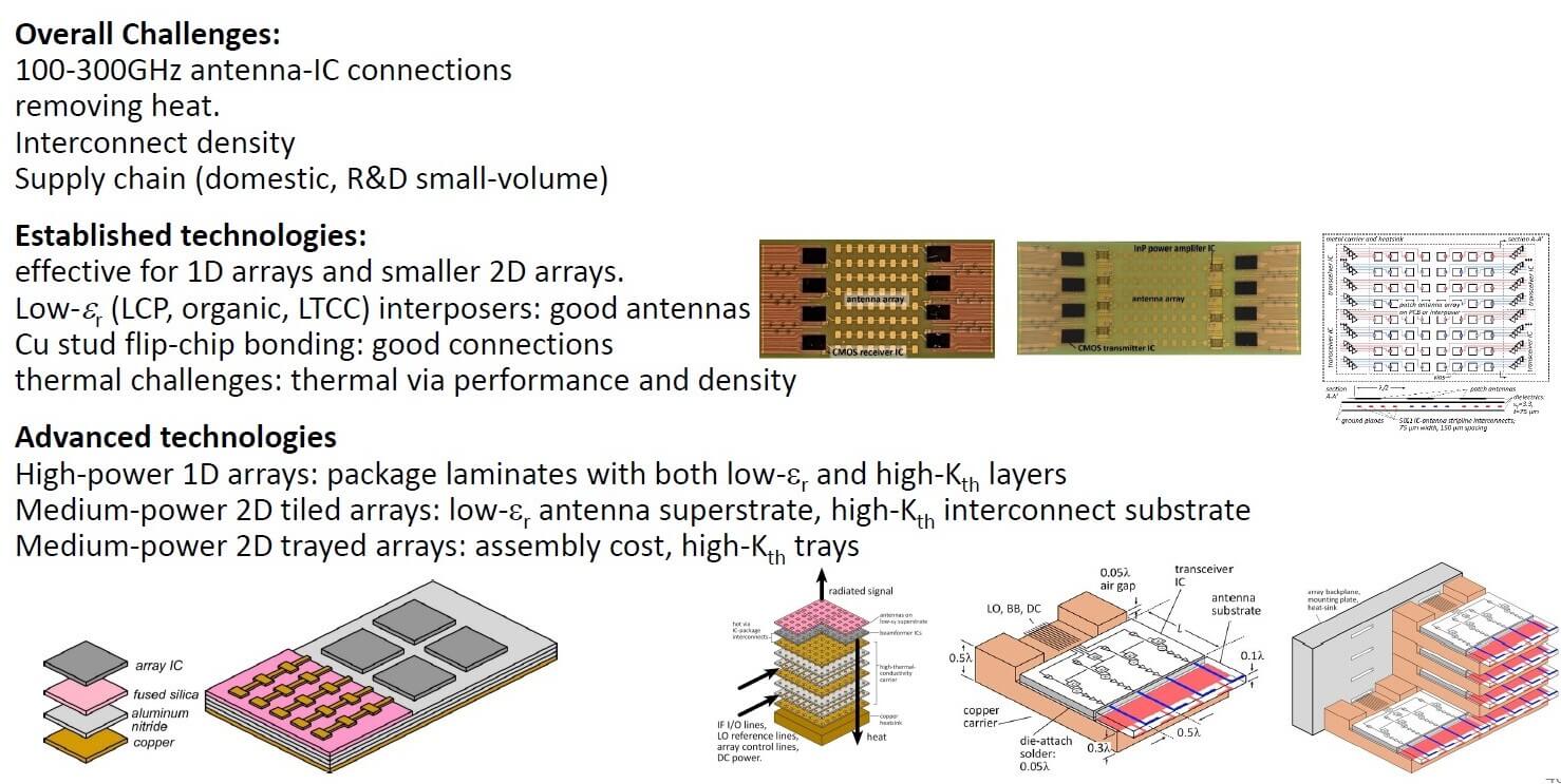
Mark Rodwell of UCSB gave a presentation on “Packaging Challenges in 100-300GHz wireless” While Rodwell’s presentation was a review of high-frequency wireless, he did cover some basics on materials and configuration requirements for high-frequency packaging (Figure 5)
The most important thing he said was his call for a “MOSIS equivalent” for advanced packaging options so academics especially can access the latest advanced packaging options.

Tohoku Univ, JCU Corp, and T-Miro Collaboration
A Group of Japanese institutes and companies reported on their studies on copper morphology effects on cu-cu hybrid bonding.
They found that if they enlarged (10-20um) Cu grain size in standard electroplated copper films (5µm thick) by annealing, the post-processed Cu film contains not only larger grains, but also has a relatively oriented microstructure. This appears to be important for Cu-diffusion during Cu-to-Cu direct/hybrid bonding. Tensile test data revealed that Cu-grains are 40% less strained in high-temperature annealed films. It is also inferred from Vickers hardness that larger Cu-grains were 50% softer in the resulting Cu-film. In line with both tensile test and Vickers hardness results, these Cu-Cu direct bonded samples are free from any interface across the boding region. Thus, this modified Cu-electroplating followed by post-processing is ideal to realize the low resistance Cu-Cu interconnection at the inter-chip level with a high yield.
Siemens EDA – Chip Design Exchange
Anthony Mastroianni, Director of Siemens EDA (formerly Mentor) discussed the results of the chiplet design exchange. The Chiplet Design Exchange (CDX) is a working group under the Open Domain-Specific Architecture (ODSA) sub-project under the direction of the Open Compute Project Foundation (OCP). The CDX group is comprised of members from EDA vendors, chiplet providers, and SiP end-users charted to recommend standardized chiplet machine-readable models and workflows to facilitate a chiplet ecosystem.
Successful deployment of chiplet-based devices will require the adoption of standardized chiplet models to establish this emerging ecosystem. The models proposed in this presentation are targeted to be developed by the prospective chiplet providers and delivered to their end-users. Although it will take some time before the newly proposed models are formally adopted as standards, most should be usable in their current state. EDA vendors will also need to support these models in their tools and workflows.
In addition to the proposed chiplet models, new standards for 2.5 and 3D assembly rules require new standards and formats. EDA vendors and 2.5D/3D manufacturing vendors are currently collaborating on these new standards, which will hopefully be in place by the time the chiplet ecosystem becomes available to the broader market.
For all the latest on Advanced Packaging stay linked to IFTLE………………


