
Building a state-of-the-art integrated circuit takes a lot of resources. Water, energy, chemicals, gases, and silicon wafers are just a few of the key elements required to build a chip. According to Scotten W. Jones at IC Knowledge LLC, there are 600 to 800 process steps at 5nm depending on the company, not counting inspection and metrology steps. The number of process steps will grow as the industry continues to shrink to 2nm and possibly below. As the number of process steps increases, the level of resources, especially power and water, needed to produce ships continues to increase. How does the semiconductor industry improve sustainability in the semiconductor fab while meeting the worldwide demand for integrated circuits?
The Lithography Challenge
As the industry moves deeper into 5nm, the advanced lithography steps have shifted from 193i using multiple patterning steps, along with a significant number of etch and deposition steps, to extreme ultraviolet (EUV) lithography, which reduces the number of lithography and deposition and etch steps needed to manufacturer the wafer. Sam Wang, VP of Research at Gartner states that TSMC is using 87 mask layers for the 7nm DUV process. 79 mask layers for the 7nm EUV process, of which 4 are EUV, and the 5nm process is 81 mask layers 14 of them are using EUV.
The reduction of mask steps is good news from a sustainability perspective, as it also reduces the number of etch, deposition, and cleaning steps that are associated with multiple patterning. The bad news is that EUV lithography is much more energy-intensive than 193i lithography processing, even with more process steps.
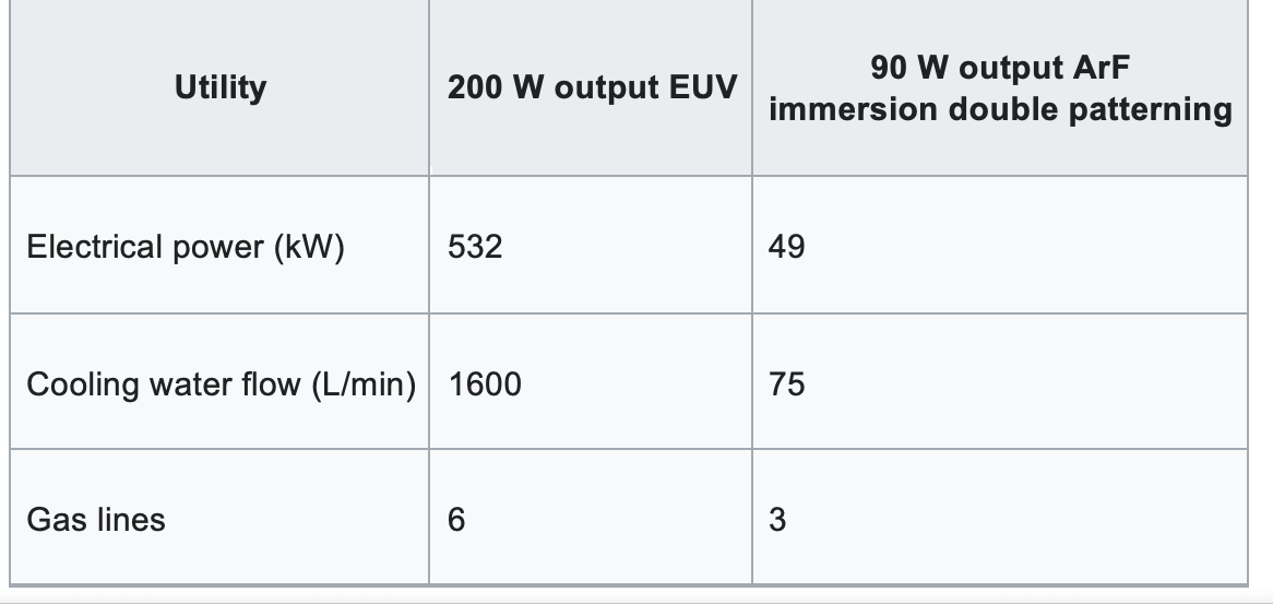
Figure 1 shows information presented in 2008 at the Sematech symposium in Japan, demonstrating that EUV uses 10x the power of DUV lithography. More recent data in a Laser Focus World post written by Andres Thoss, suggests each EUV system uses a Megawatt (MW) of power. A Taiwanese news company reports that TSMC with 30 EUV machines is estimated to use 900,000-kilowatts of energy per day. As a side note, this might be one reason TSMC is looking offshore for new factories, as the Taiwan energy infrastructure might have difficulty supporting the amount of energy needed to support EUV expanded EUV production, especially with TSMC’s sustainability goals.
Even with the reduced number of process steps, it is unlikely power parity would be reached between EUV and DUV processes. However, 7nm and below transistors cannot be manufactured without EUV; thus, the process engineers will need to look at other areas for sustainability.
Thermal Budget
Another plus for more sustainable semiconductor fabs is the reduction of the thermal budget in process flows for advanced integrated circuits. Processes and equipment have evolved over time moving from batch equipment to either single wafer or batch systems. CVD, epitaxy, and oxidation diffusion; all high-temperature processes historically performed in a tube furnace, or a bell jar, have transitioned in many cases to single wafer tools.
Depending upon the process, either a constant temperature substrate is used, or a lamp system that can heat up and cool down rapidly. New precursors have enabled lower deposition temperatures, and the use of ALD has reduced deposition temperatures even further.
Oxidation diffusion furnaces have transitioned to single wafer systems, except in cases where the cost of ownership of a tube furnace outweighs that of the single wafer advantages. In many cases the diffusion process has moved from using a heat source to rapidly heat the wafer to a laser that heats only the upper layers, thus not impacting dopant layers that have already been annealed, and potentially reducing the amount of energy needed to heat each wafer.
The positives of single wafer tools have been touted for several years. Better on wafer temperature uniformity, gas distribution, and typically better uniformity than a batch system can deliver. The potential negatives are that you have to have more tools to deliver the same number of wafers as a batch system, which could possibly require more energy. Additionally, more steps per node will require in some instances additional tools per fab also increasing the energy budget.

To a more Sustainable Sub-Fab
A recent blog by Jim L’Heureux, Andreas Neuber, Ph.D. of Applied Material (AMAT) describes a software framework and network of controllers that gather data from both the tools and the sub-fab equipment so intelligent decisions can be made about operations and energy use. This tool can be connected to up to four pieces of equipment in the sub-fab. In this example, they demonstrate how it can be connected to vacuum pumps and an abatement system which is typical for CVD and etch tools in a fab. According to the authors, iSystem is a
Typically, sub-systems operate at full power when the fab tool is idle. AMAT’s tool allows the sub-fab tools to match the process flow in the fab tool. TSMC is using it as part of its sustainability effort. The graphic below shows how TSMC has the tool set up to monitor point-of-use sub-system tools.
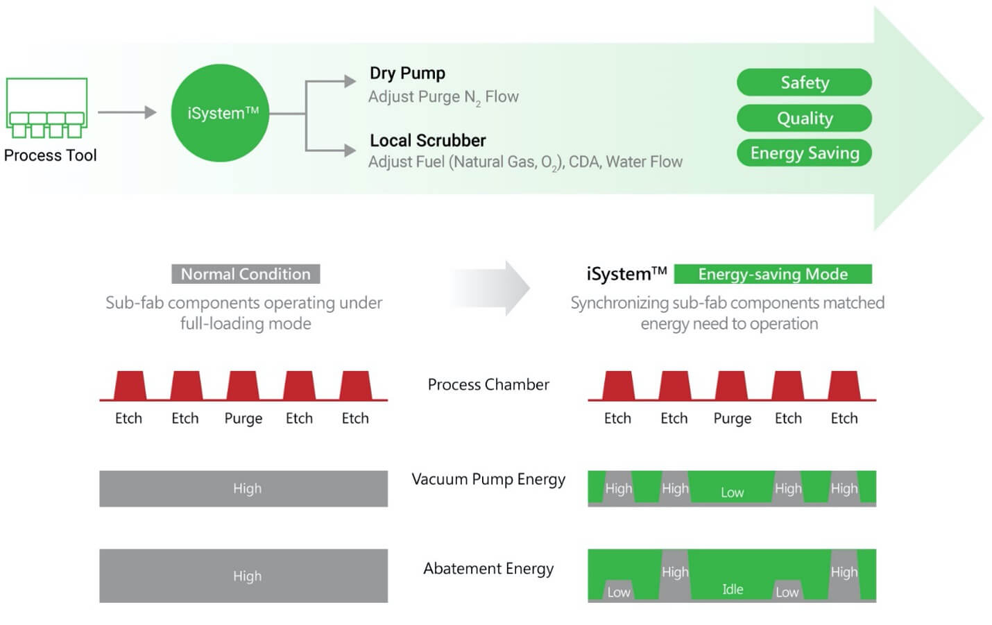
Results to date, according to the AMAT blog, saves TSMC 13.4 million kilowatt-hours of electricity annually while reducing carbon emissions by 13,800 tons. TSMC is in the process of implementing the iSystem across the fab as part of its sustainablility program. It will be interesting to see how much energy this saves per fab, and what the impact is on the carbon footprint when it is fully implemented.
The above is a start but there is still a long way to go in reducing a fabs sustainability footprint.
Feature image source: Taiwan Semiconductor Manufacturing Co., Ltd.


