
Can the USA wrestle back Front- and Back-end Semiconductor Manufacturing?
Humpty Dumpty
Humpty Dumpty sat on a wall
Humpty Dumpty had a great fall
All the king’s horses and all the king’s men
Couldn’t put Humpty together again
Recently, Congress has been tossing ideas about investing $Bs into the high technology sector with several bills:
- The Chips for America Act focused on re-shoring
- The Facilitating American-Built Semiconductors (FABS) Act promises tax credits for investments in either equipment or fabs
- Then another $250 billion US Innovation and Competition Act, which earmarks $52bn for new chip manufacturing and research
All are trying to address the chip shortage that has hit the world.
Chip shortages are nothing new and have happened since the 1980s. However, regardless of the reasons of the shortage, within a 2-year period, the chip demand vs. supply balanced out.
In 1980, if you wanted to work with silicon, your options were the large integrated device manufacturers (IDMs) that existed. Common names such as Intel, Motorola, IBM, Fairchild, TI, National Semiconductor, AMD, Cypress Semiconductor, Mostek, etc. Many were based in either Silicon Valley with a few in the Boston area and both Austin and Dallas, Texas. Many of these companies no longer exist due to mergers and acquisition (M&A) activities or bankruptcy.
My initial reaction to the various Congress plans was: It is about time!
After some consideration, I started to think about the changes over the 40+ years and re-examined my perspective. I have tried to summarize whether the semiconductor system is broken a la Humpty Dumpty.
A Look Back
Back in 1979, semiconductor sales were about $10B worldwide. By 2020, this had grown to $466.2 billion, just under 10% CAGR for this timeframe.
Back in the 1980s, the market included IDMs and system houses.
IDMs were responsible for a wide range of activities:
- market research on what products to design/sell
- what selling price and support to provide (documentation, application support, etc.)
- most likely an internal computer-aided design (CAD) group creating/modifying various software to aid design and verification of integrated circuits
- design/layout/verification of their designs using internally developed tools
- producing reticles/masks
- silicon/wafer process design and fabrication
- assembly/test/branding/QA
and

- shipping to their end customers
The IDM business model was a barrier to entry for potential new IDMs due to large staff, owning fabrication site(s), huge expenses, and a high-risk factor that makes them responsible for everything. If one of the IDM’s functional groups failed to perform, the entire ‘ship’ could sink. The biggest decision was when to build a new fab and how quickly it could be filled with paying customers. Fabs that had low utilization (under 80%) posed a significant financial risk for the owner.
The system houses built all the products that consumers purchased using various suppliers’ products including standard products from IDMs. IDM’s products were similar to the Ford’s Model T, where you could purchase any COLOR car as long as it was black. The early integrated circuits were not customized based on the end users’ needs.
By the 1984-1995 time period, the IDM model was destroyed because of two strategies:
- A comparative advantage in which products/services are purchased from regions with lower costs and acceptable quality (this is a cost decision). This can be replaced when another region can perform at lower costs. Examples include Outsourced Assembly and Test (OSAT) companies primarily located in Asia.
- A competitive advantage from any internal function that a company can hone into consistently outperforming their competitors. Example: TSMC as a Foundry.
What resulted by 1995?
Many customers were offered application-specific integrated circuits (ASICs), for which the end customers could determine what functionality was integrated rather than using off-the-shelf standard products. ASICs were built upon predefined library elements that removed all the manual physical layout required to create a design. Now, the task had elevated to metal wiring between these blocks using place-and-route (P&R) software.
- Electronic design automation (EDA) software was developed and supported by independent companies that provided design and verification tools to anyone. Companies no longer needed to create large internal CAD groups.
- Silicon intellectual property (SIP) was offered by various 3rd party vendors (besides silicon vendors) that had predefined functionality supported by models and physical layout. This significantly reduces the workforce and hours developing and characterizing these elements.
- OSAT companies offered as a service no longer requiring in-house, high-volume manufacturing.
- The more difficult and expensive front-end wafer fabrication outsource model was driven by Morris Chang and Taiwan through TSMC.
Within two decades, the old IDM model was no longer required and was extinct. These changes produced the following results:
- Fabless companies that could purchase all the services required to create silicon customized exactly how they wanted it sprung up everywhere
- IDMs re-evaluated where and how they could add value:
- Some decided to focus on niche areas that required tight integration between their designs and wafer fabrication. Notable examples: Intel and CPUs; TI and analog functionality; On Semi and analog functionality; Micron and memories. Even these ‘IDMs’ have jettisoned functional areas that they could easily purchase from other suppliers such as CAD groups (EDA), internal packaging (OSATs), etc.
- Others decided to migrate to a fabless business model and sell off any high-volume manufacturing. A notable example: AMD
- Others decided to elevate to higher levels of products and services selling off their high-volume manufacturing. A notable example: IBM
- The IDM barrier to entry was significantly lowered for any company desiring silicon within their product.
- The EDA tools and SIP also enabled many more job opportunities for people, and they were no longer restricted to the old IDMs and their locations.
How has this affected US chip manufacturing capacity?
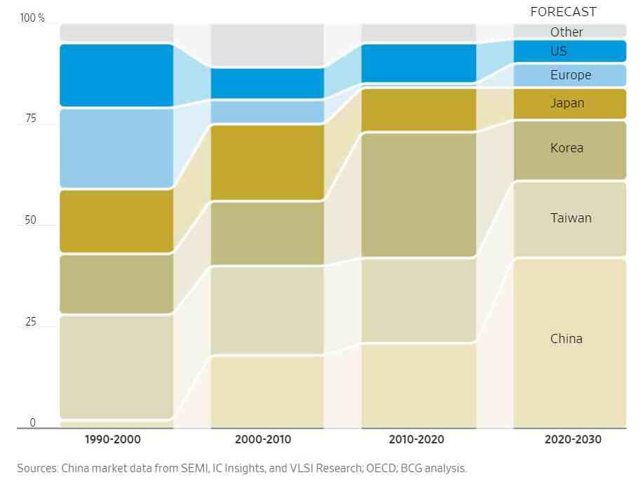
Given that much of the world is now fabricating wafers, the US dominant position in 1980 has continued to shrink down to ~12% (Figure 1). But capacity is only one factor, which is meaningless unless you dig deeper into the process nodes, yields, equivalent wafers produced, and types of designs that are manufactured.
Was the US high-tech industry successful?
Looking at the demise of US IDMs, you might state that it was a huge failure. But the world has evolved with many more engaged in generating products and sharing in the profits from these activities. Figure 2 represents the worldwide semiconductor manufacturing by process nodes. Back in 1980, the state of the art was 5µm which is 1000x larger than today’s 5nm node.
Any process node smaller than 14nm comes from either TSMC, Samsung, or Intel. All the others are various niche players, which does not mean they are financially small. All of these foundries and OSATs raise the local country’s standard of living. You might ask about the impact on US engineers and their jobs? Well, there are many more fabless companies hiring semiconductor engineers now than the IDMs that existed in 1980. There are many more companies and locations where you can work and live besides Silicon Valley.
But what about national security?
National security is a different area that requires much more analysis and planning than just throwing billions of dollars at the US high technology sector. Taiwan had the right situation and the right individual that could achieve success. In my opinion, Taiwan’s goal was more definitive, better planned, and spread out over a long-time span. If the US government is serious about infusing lots of cash into ‘the system’, it might be better off to agree on more specifics and expected results and timeframes.
A short summary over 40 years of progress:
- $500B and growing semiconductor sales per year from $10B in 1980.
- 1000x smaller geometries that can be manufactured than in 1980.
- Many more product development companies exist creating all types of products that use semiconductors, including greeting cards!
- Processing and memory capabilities that allow individuals to carry more compute power, music, web browsing, email, and phone contacts than in 1980.
Is Humpty Dumpty broken?
Absolutely and ALL of us are in a better place. ~ Bill Martin